Download
1 / 1
10 likes | 245 Views
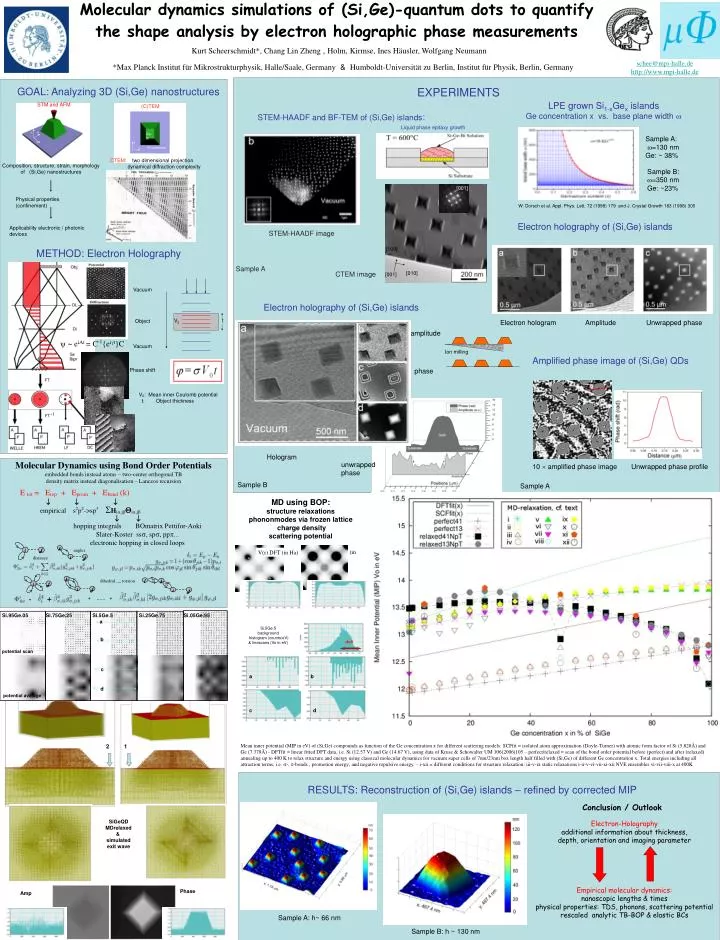
Molecular dynamics simulations of (Si,Ge)-quantum dots to quantify the shape analysis by electron holographic phase measurements. Si.95Ge.05. Si.75Ge.25. Si.5Ge.5. Si.25Ge.75. Si.05Ge.95. GOAL: Analyzing 3D (Si,Ge) nanostructures. a. Electron holography of (Si,Ge) islands.

E N D
Molecular dynamics simulations of (Si,Ge)-quantum dots to quantify the shape analysis by electron holographic phase measurements Si.95Ge.05 Si.75Ge.25 Si.5Ge.5 Si.25Ge.75 Si.05Ge.95 GOAL: Analyzing 3D (Si,Ge) nanostructures a Electron holography of (Si,Ge) islands Amplified phase image of (Si,Ge) QDs STM and AFM (C)TEM b j amplitude i z y 2 1 j j potential scan Vacuum x k Ge-Si j i y c k i x Si substrate phase V0 t Object i d j CTEM: two dimensional projection dynamical diffraction complexity potential average SiGeQD MDrelaxed & simulated exit wave Composition, structure, strain, morphology of (Si,Ge) nanostructures Vacuum Si.5Ge.5 background histogram (counts/eV) & linescans (Vo in eV) angles -4eV Phase shift distance CBED Physical properties (confinement) l k V0: Mean inner Coulomb potential t: Object thickness a b Phase i Hologram Amp 10 amplified phase image Unwrapped phase profile dihedral ,,,, torsion EELS unwrapped phase Applicability electronic / photonic devices c d + + ...... + Sample B Sample A = V(r)BOP (in eV) V(r) DFT (in Ha) Kurt Scheerschmidt*, Chang Lin Zheng , Holm, Kirmse, Ines Häusler, Wolfgang Neumann schee@mpi-halle.dehttp://www.mpi-halle.de *Max Planck Institut für Mikrostrukturphysik, Halle/Saale, Germany & Humboldt-Universität zu Berlin, Institut für Physik, Berlin, Germany EXPERIMENTS LPE grown Si1-xGex islands Ge concentration x vs. base plane width w STEM-HAADF and BF-TEM of (Si,Ge) islands: Liquid phase epitaxy growth Sample A: =130 nm Ge: ~ 38% Sample B: =350 nm Ge: ~23% [001] W. Dorsch et al. Appl. Phys. Lett. 72 (1998) 179 and J. Crystal Growth 183 (1998) 305 Electron holography of (Si,Ge) islands STEM-HAADF image [100] METHOD: Electron Holography Sample A [010] CTEM image [001] Electron hologram Amplitude Unwrapped phase y ~ eiAt = C-1{eigt}C Sample A Si Ion milling Molecular Dynamics using Bond Order Potentials embedded bonds instead atoms – two-center orthogonal TB density matrix instead diagonalisation – Lanczos recursion E tot = Erep + Eprom + Eband (k) MD using BOP: structure relaxations phononmodes via frozen lattice charge density scattering potential empirical s2p2->sp3SHia,jbQia,jb hopping integrals BOmatrix Pettifor-Aoki Slater-Koster sss, sps, ppp... electronic hopping in closed loops Mean inner potential (MIP in eV) of (Si,Ge) compounds as function of the Ge concentration x for different scattering models: SCFfit = isolated atom approximation (Doyle-Turner) with atomic form factor of Si (5.828Å) and Ge (7.378Å) - DFTfit = linear fitted DFT data, i.e. Si (12.57 V) and Ge (14.67 V), using data of Kruse & Schowalter UM 106(2006)105 – perfect/relaxed = scan of the bond order potential before (perfect) and after (relaxed) annealing up to 400 K to relax structure and energy using classical molecular dynamics for vacuum super cells of 7nm/23nm box length half filled with (Si,Ge) of different Ge concentration x. Total energies including all attraction terms, i.e. s-, p-bonds , promotion energy, and negative repulsive energy. – i-xii = different conditions for structure relaxation: iii-v-ix static relaxations i-ii-v-vi-vii-xi-xii NVE ensembles vi-vii-viii-x at 400K RESULTS: Reconstruction of (Si,Ge) islands – refined by corrected MIP Conclusion / Outlook Electron-Holography additional information about thickness, depth, orientation and imaging parameter Empirical molecular dynamics: nanoscopic lengths & times physical properties: TDS, phonons, scattering potential rescaled analytic TB-BOP & elastic BCs Sample A: h~ 66 nm Sample B: h ~ 130 nm