Download
1 / 43
430 likes | 645 Views
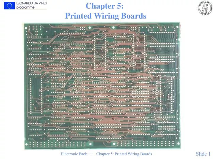
Chapter 5: Printed Wiring Boards. Substrate. The purpose of the substrate for electronic component mounting is: Mechanical support Electrical interconnection Heat conduction. Organic Substrate: Printed Wiring Boards (PWB). Requirements: Electrical properties Mechanical properties

E N D
Chapter 5: Printed Wiring Boards Electronic Pack….. Chapter 5: Printed Wiring Boards
Substrate • The purpose of the substrate for electronic component mounting is: • Mechanical support • Electrical interconnection • Heat conduction Electronic Pack….. Chapter 5: Printed Wiring Boards
Organic Substrate: Printed Wiring Boards (PWB) • Requirements: • Electrical properties • Mechanical properties • Chemical resistance • Fire resistance • Processability • Adhesion • Low moisture absorption Fig. 5.1: Woven glass fibre for printed wiring board reinforcement Electronic Pack….. Chapter 5: Printed Wiring Boards
Printed Wiring Boards, continued Table 5.1: Conventional laminates for printed wiring boards. (The designations are according to National Electrical Manufacturers Association, NEMA, USA.) Electronic Pack….. Chapter 5: Printed Wiring Boards
Printed Wiring Boards, continued Fig. 5.2: Printed wiring board structures with varying complexity: a) Single sided and double sided.b) Double sided through hole plated with bare Cu or Sn/Pb surface.c) Four layer board.d) Six layer board with two Cu/Invar/Cu cores. Electronic Pack….. Chapter 5: Printed Wiring Boards
Printed Wiring Boards, continued • Generation of Design Data, Photo- or Laser Plotting Fig. 5.3: Photo plotter, schematically. Electronic Pack….. Chapter 5: Printed Wiring Boards
Single Sided Boards • 1. Drilling / punching of registration holes • 2. Panel cleaning • 3. Printing of etch resist • 4. Etch ing • 5. Stripping • 6. Printing solder resist • 7. Curing of solder resist • 8. Cleaning of solder areas • 9. Deposition of solder coating • 10. Punching of holes and edge countour (or drilling/milling)This is a substractive process • Alternative: Additive processes Electronic Pack….. Chapter 5: Printed Wiring Boards
Single Sided Boards, continued Fig. 5.4: Process steps of "print and etch" process for single sided boards Electronic Pack….. Chapter 5: Printed Wiring Boards
Double Sided ThroughHole Plated Boards • 1. Drilling • 2. Cleaning • 3. Activation for chemical plating • 4. Chemical plating • 5. Electrolytic plating • 6. Pattern definition • 7. Tin/lead masking plate • 8. Etching • 9. Fusing • 10. Organic solder resist Electronic Pack….. Chapter 5: Printed Wiring Boards
Double Sided ThroughHole Plated Boards, continued Fig. 5.5: Through hole plated PWB, process steps: a) Panel plating. b) Pattern plating. c) Hot air levelling. Electronic Pack….. Chapter 5: Printed Wiring Boards
Double Sided Through Hole Plated Boards:Choice of Surface Metallisation and Solder Resist Fig. 5.6.a: Selective Sn/Pb surface coverage with hot air levelling. The alternatives, bare Cu or Sn/Pb on all Cu surface, are shown in Figure 5.2 b). Electronic Pack….. Chapter 5: Printed Wiring Boards
Choice of Surface Metallisation and Solder Resist, continued Fig. 5.6.b: "Tenting", i.e. covering of the via holes by dry film solder resist. Electronic Pack….. Chapter 5: Printed Wiring Boards
Multilayer Printed Wiring Boards • 1. Drilling • 2. Rinse, Photo process for inner layers • 3. Etch inner layers • 4. Black oxidation for adhesion promotion • 5. Baking • 6. Lamination • 7. Drilling of through holesFurther process as for double layer boards Electronic Pack….. Chapter 5: Printed Wiring Boards
Multilayer Printed WiringBoards, continued Fig. 5.7: Process steps for multilayer printed wiring boards with holes only through the board. Electronic Pack….. Chapter 5: Printed Wiring Boards
Multilayer PrintedWiring Boards, continued Fig. 5.8: Types of via holes: a) Through hole. b) Buried hole. c) Blind hole. Figure d) shows a microscope section of a drilled blind via. (Contrave´s "Denstrate" process). Electronic Pack….. Chapter 5: Printed Wiring Boards
Fine Line PrintedWiring Boards, additive process Fig. 5.9 a): The development of minimum line width from 1965 until 1990. The figures in the ovals tell how many conductors can be positioned between the leads of DIP-components with a lead pitch of 0.1" (number of "channels"). Electronic Pack….. Chapter 5: Printed Wiring Boards
Fine Line PrintedWiring Boards, additive process, continued • Etch control: Under etch/etch factor • Additive process • Clean-room • Collimated light. Fig. 5.9 b): Underetch and etch factor. Electronic Pack….. Chapter 5: Printed Wiring Boards
Fine Line Printed Wiring Boards: Photolithographic Process Fig. 5.10.a: Machine for double sided illumination with parallel light, for pattern transfer from photographic film for fine line printed wiring boards. Electronic Pack….. Chapter 5: Printed Wiring Boards
Fine Line Printed Wiring Boards: Photolithographic Process, continued Fig. 5.10.b : Automatic in-line system for lamination of photoresist, illumination and development, in an enclosed clean room atmosphere. Electronic Pack….. Chapter 5: Printed Wiring Boards
Metal Core Printed Wiring Boards • Better heat conduction • TCE matching with ceramic packages • Most common: Cu/Invar/Cu Fig. 5.2.d) Six layer board with two Cu/Invar/Cu cores. Electronic Pack….. Chapter 5: Printed Wiring Boards
Metal Core Boards, continued Fig. 5.12 a): Cross section of metal core board with one Cu/Invar/Cu core (Texas Instruments). Fig. 5.12 b): Thermal coefficient of expansion of Cu/Invar/Cu, as function of the composition (Texas Instruments). Electronic Pack….. Chapter 5: Printed Wiring Boards
New Materials for PWBs • Higher Tg • Better dimensional stability • er low, not dependent on T, f, or moisture • Low losses • Lower TCE • Purpose • High frequency use • Controlled characteristic impedance • High reliability • Materials • Cyanate ester • PTFE (Teflon) • Polyimide • and others Electronic Pack….. Chapter 5: Printed Wiring Boards
New Materials for PWBs,continued Fig. 5.13: TCE for FR-4 below and above Tg in a): the x or y direction, b): the z-direction Electronic Pack….. Chapter 5: Printed Wiring Boards
New Materials for PWBs,continued Table 5.2: Material parameters for polymers for printed wiring boards Electronic Pack….. Chapter 5: Printed Wiring Boards
New Materials for PWBs,continued Fig. 5.14: Frequency dependence of er and tan d for FR-4.er :Relative dielectric constant. tan d: Loss tangent. Electronic Pack….. Chapter 5: Printed Wiring Boards
Commercial Products Table 5.3: Materials parameters for important materials combinations and some commercial products for high performance printed wiring boards. Electronic Pack….. Chapter 5: Printed Wiring Boards
Commercial Products,continued Fig. 5.15 a): Structure of Rogers material RO2800. Electronic Pack….. Chapter 5: Printed Wiring Boards
Commercial Products,continued Fig. 5.15 b): Combination of Gore-Ply and FR-4 gives a simple process, and at the same time low dielectric losses and reduced capacitance to ground. Electronic Pack….. Chapter 5: Printed Wiring Boards
Commercial Products,continued Fig. 5.16: Attenuation in (dB) as function of frequency for a one meter long stripline, for the high performance materials Gore, Nelco and polyimide, compared to FR-4. Electronic Pack….. Chapter 5: Printed Wiring Boards
Commercial Products,continued Fig. 5.17: Top: Microwire from PCK, with conductors insulated with organic insulation, and a metal foil as ground plane. Bottom: Next generation technology, where each conductor has its own metal shield. Electronic Pack….. Chapter 5: Printed Wiring Boards
Commercial Products,continued Fig. 5.18: The equipment head that deposits the conductors on the laminate for Microwire. Electronic Pack….. Chapter 5: Printed Wiring Boards
Special Boards • Flexible printed wiring boards • Dynamic or static bending. • Uses: Movable parts and odd shaped, cramped places Electronic Pack….. Chapter 5: Printed Wiring Boards
Flexible PrintedWiring Boards, continued Fig. 5.19: Flexible printed wiring boards: Most of the electronics in Minoltas camera Maxxum 9000 is on two flexible printed circuit boards. Electronic Pack….. Chapter 5: Printed Wiring Boards
Flexible PrintedWiring Boards, continued Table 5.4: Properties for materials used for flexible printed wiring boards. Electronic Pack….. Chapter 5: Printed Wiring Boards
Flexible PrintedWiring Boards, continued Fig. 5.20: Cross section of flexible PWB: Top: Single layer conductor foil. Bottom: Double layer conductors with through hole plating. Electronic Pack….. Chapter 5: Printed Wiring Boards
Membrane Switch Panels • Purpose: Switches and informative instrument fronts. Fig. 5.21 a): Membrane switch panel, schematically.Top: Structure Bottom: Cross section of a normal panel and a panel with metal dome. Electronic Pack….. Chapter 5: Printed Wiring Boards
Membrane Switch Panels,continued Fig. 5.21 b): Exploded view of simple switch panel Electronic Pack….. Chapter 5: Printed Wiring Boards
3 D Moulded Boards • Combine substrate and chassis, integrated stand-offs, etc. • Materials: • Polysulphone, polyetherimide, etc. Electronic Pack….. Chapter 5: Printed Wiring Boards
3 D Moulded Boards, continued Table 5.5: Materials used for moulded circuit boards, and their properties, compared to epoxy and polyimide Electronic Pack….. Chapter 5: Printed Wiring Boards
3 D Moulded Boards, continued Fig. 5.22.a: 3 dimensional moulded component carrier in a telephone application. Electronic Pack….. Chapter 5: Printed Wiring Boards
3 D Moulded Boards, continued Fig. 5.22.b: 3 dimensional moulded component carrier in a power supply application. Electronic Pack….. Chapter 5: Printed Wiring Boards
3 D Moulded Boards, continued Fig. 5.23: The process for moulding of a 3-dimensional substrate with Cu conductor patterns deposited on a temporary film. Electronic Pack….. Chapter 5: Printed Wiring Boards
3 D Moulded Boards, continued Fig. 5.24: Two steps moulding process for preparation for chemical plating of the conductor pattern on 3-D component substrates. The first moulding is done with a catalytically activated plastic, the second with "passive" plastic, where chemical plating is not sticking. (PCK, USA). Electronic Pack….. Chapter 5: Printed Wiring Boards