Download
1 / 19
190 likes | 218 Views
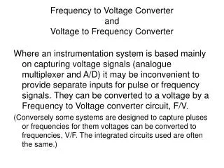
This outline covers the original and modified designs of a resistance to frequency converter. It also details component parts, buffer optimization, design specifications, and conclusions. The design focuses on chemiresistive sensors and their application in detecting gas concentrations, addressing layout challenges, buffer optimization, and power dissipation considerations.

E N D
Resistance to Frequency Converter Amol Mupid Andrew Ricketts
Outline • Original design • Component parts • Roadblock • Modified design • Buffer optimization • Design specification • Conclusion
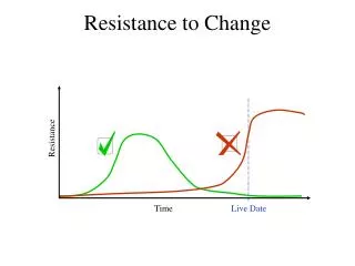
Chemiresistive Sensors Rs : resistance of nanowire C : concentration of the gas A,α : constants that change with type of gas and temperature Rs 400 350
- + + - Original design C R3 Vout D Q R2 R5 Qbar CLK R1 R4 Rs
Original design components • Diode • Spice simulation • …but layout issues insurmountable
Original design components • Zener Diode • More simulations possible • …but layout even more challenging
Modified design • Key point is that what is desired is a way to control oscillations based on input voltage • Voltage Controlled Oscillator (VCO) • Buffer added to output to ensure rapid rise and fall of output • square wave
VCO design • LC tank oscillators • Good phase noise with low power • but tuning range is relatively low • Output frequency may fall out of range due to process variations • Spiral inductors occupy a lot of area, high cost and low yield issues. • Ring oscillators • Easy integration, high yield, low cost. • Less chip area • In-phase outputs
Buffer optimization • Initial single stage buffer • Moved output close to binary • Had difficulty clamping small swings about origin • Double stage buffer • Delay increase inconsequential • Greatly improved clamping range
Transistor sizing Core area 48.75 X162.6 = 7,926(um^2)
Resistance • We want the Vcontrol be to be in between operable range • => Rs*VDD/ (Rs+ R) has to be in between 3.3V and 5V R Vcontrol Rs
Conclusion • The change in the sensor resistance can be detected in “ns” range and converted to square wave pulses • This completely eliminates the need of ADC, huge potential resource savings. • Successfully overcame practical design issues and produced desired results.
Thank You Questions??