Download
1 / 57
640 likes | 1.42k Views
Properties, Characterization, and Applications of Carbon Nanotubes. Y. Tzeng Auburn University Alabama USA July 2003. Outline. CNT’s Properties Mechanical Properties Electrical Properties Other Properties Characterization of CNTs SEM, TEM, AFM Raman, EELS Manipulating CNTs

E N D
Properties, Characterization, and Applications of Carbon Nanotubes Y. Tzeng Auburn University Alabama USA July 2003
Outline • CNT’s Properties • Mechanical Properties • Electrical Properties • Other Properties • Characterization of CNTs • SEM, TEM, AFM • Raman, EELS • Manipulating CNTs • Applications of CNTs
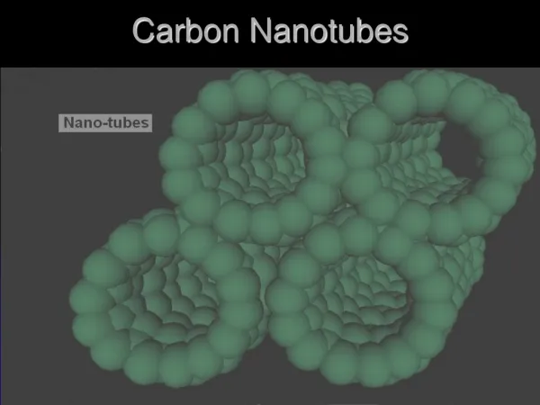
Helicity and sp2 Bonding • Single-Walled Nanotubes (SWNTs) vs. Multi-Walled Nanotubes (MWNTs) • Large Variety of Chiral Angles ⇨ Armchair, Zigzag, and Helical • Quasi-one Dimensional Hollow Tube • Extremely High Aspect RatioD: 1- 50 nm, L: 1-100 μm • Strong sp2 Bonding Otto Zhou, ADC/FCT 2001
CNTs’ Properties • Electrical properties depend on geometry of nanotube • Roughly 2/3 are semiconductors and 1/3 are metallic in random growth • Tremendous current carrying capacity 1 billion Amps/cm2 , electromigration not an issue • Excellent heat conductor twice as good as diamond • High strength much higher than high-strength steel Young Modulus ~ 1 TPa (SWNT) and 1.25 TPa (MWNT) (Steel: 230 GPa) High Aspect Ratio: 1000 – 10,000 Density: 1.3 – 1.4 g/cm3 Maximum Tensile Strength: 30 GPa Thermal Conductivity: 2000 W/m.K (Copper has 400 W/m.K)
k 3000 VTE Sensing coil ~T2 Heating coil 14 nm multiwall (MW) carbon nanotube (CN) I Thermal Property of CNT
2.1 Electrical properties of CNTs • Four probes made of tungsten • MWCNT • 0.051 -m ~ 8 m-m • Structure dependant • Forced contact (e-beam) • Four pre-patterned Au fingers • MWCNT powders in solution • 0.35 ~ 2.6 k Ref. T.W. Ebbesen et al., Nature 382, 54, 1996 A. Bachtold et al., Appl. Phys. Lett., 73, 2, 1998 YC
SWCNT Crossbars Electric field assisted deposition and orientation of the nanowires was accomplished by patterning two parallel electrodes with a 10 um gap onto a silicon wafer coated with 0.5 um SiO2. This device was immersed in a suspension of SWNTs dispersed in a solution that contained 0.4 mL of ODCB and 100 mL of CHCl3. An AC field was generated by applying a 20 Vp-p AC voltage at 4 MHz for a period of 4 to 15 minutes while the solution was stirred. After deposition, the electrode was chemically etched away, and a new electrode set was deposited perpendicular to the first set. The process repeats. http://www.its.caltech.edu/~heathgrp/papers/Paperfiles/2002/diehlangchemint.pdf
Nanotube Conductance • Semiconducting when (m, n) indices: m – n ≠ 3 x integer • Rest are metallic. • Carbon Nanotubes are intrinsically P-Type semiconductors. • Energy band gap can be affected by increasing the magnetic field along the axis • Band gap of a semiconducting nanotube proportional to 1 / diameter, • e.g.,1.6 nm Nanotube band gap ~ 0.6 eV • Φ~ 4.5 eV < most contact metals (Au or Pt)
CNT Conductance Variation Change of electrical resistance of SWNT with exposure to O2 Collins et al., Science (2000); Kong et al., Science (2000)
Quantum Effect • Conductance appears to be ballistic over micron scales, even at room temperature. • Ballistic = no dissipation in the tube itself = very high current densities are possible. Frank et al., Science 280, 1744 (1998).
5.2 Experimental apparatus of the electrical contact measurement setup Top electrode: CNT coated loop Bottom electrode: CNT coated substrate Replace Au wire with CNT coated loop Current limiting resistance: 5 k Voltage: 10Vp-p, 60Hz YC
5.3.1 Contact resistance between CNT coated electrodes in ambient air • Resistance dropped from thousands to ~160 Ω within 30um, consistent. • Pulling put, remained con-ductive after initial point • ~60um beyond the initial point, still conductive length of CNTs YC
Electron Field Emission From CNTs • Low turn-on electric field and threshold electric field • High field enhancement factor • High current density • High current stability, low degradation rate
http://www.cs.unc.edu/Research/nano/documentarchive/talks/2002Taiwan_taylor_SEM_AFM.pdfhttp://www.cs.unc.edu/Research/nano/documentarchive/talks/2002Taiwan_taylor_SEM_AFM.pdf
2.3 Electron field emission of CNTs • The local field will be higher by a factor , which gives the aptitude of the emitter to amplify the field and is determined by geometrical shape of the emitter. • F = E = V/d0, where E is the macroscopic field. • Current density, J = A(F2/) exp (-B 3/2/ F) • I (F2/) exp (-B 3/2/ F) with B = 6.83 109 (VeV-3/2 m-1) • For carbon film emitters, is usually taken 5 eV. Ref. J.-M. Bonard et al., Carbon, 40, 1715, 2002 YC
2.3 Electron field emission of CNTs I-V characteristics for different continuous nanotube films Emission curve for a single MWCNT with open and closed tips Closed: As-grown, purified Open: Heat treatment to open, purified Ref. J.-M. Bonard et al., Appl. Phys. A., 69, 245, 1999 YC
http://www.cs.unc.edu/Research/nano/documentarchive/talks/2002Taiwan_taylor_SEM_AFM.pdfhttp://www.cs.unc.edu/Research/nano/documentarchive/talks/2002Taiwan_taylor_SEM_AFM.pdf
http://www.cs.unc.edu/Research/nano/documentarchive/talks/2002Taiwan_taylor_SEM_AFM.pdfhttp://www.cs.unc.edu/Research/nano/documentarchive/talks/2002Taiwan_taylor_SEM_AFM.pdf
http://www.cs.unc.edu/Research/nano/documentarchive/talks/2002Taiwan_taylor_SEM_AFM.pdfhttp://www.cs.unc.edu/Research/nano/documentarchive/talks/2002Taiwan_taylor_SEM_AFM.pdf
http://www.ece.neu.edu/edsnu/mcgruer/nano/simpsonJVSTB_March%202001.pdfhttp://www.ece.neu.edu/edsnu/mcgruer/nano/simpsonJVSTB_March%202001.pdf
Cees Dekker, Delft University SEM, TEM, AFM, STM
Raman Spectra of CNTs The radial breathing mode (RBM) frequency depends on the tube diameter d as ~1/d, which allows determination of the diameter distribution from Raman spectra. Samples of SWNTS in polypropylene with different degree of nanotubes' alignment measured for three angles between the light polarization direction and fiber/tape long axis. http://www.isso.uh.edu/publications/A2001/106-iliev.htm
EELS Images of CNTs Examples of Electron Energy Loss Spectroscopy (EELS) imaging on composite nanotubes http://nlpgw.jst.go.jp/people/suenaga/kazu02.html
Manipulating CNTs with AFM Probe Kinks in tube held by Van der Walls forces on Substrate http://www.ipt.arc.nasa.gov/gallery.html
Micro-Tweezers for Nanoscale Manipulation Nanohand - for nanoscale sensing and manipulation. The gap is smaller than a micron ! Attaching a 1 micron long, 30 nm wide nanotube between two electrodes in 10 seconds. Peter Bøggild. E-mail: pb@mic.dtu.dk
Space Elevator Need 30 times stronger than steel • Carbon at least 100 times stronger • Seattle-based HighLift Systems wants to build this within 20 years
Silicon Tips vs. Carbon Nanotubes • A critical component to the AFM • Determines the force applied to the sample • Fabricated from silicon Size • 100 – 200 microns long • 10 – 40 microns wide • 0.3 – 2 microns thick • Why do we use carbon nanotube probes ? • They are long and slender • They buckle • Has a small-end diameter • Have versatile carboxylic acid tips
Silicon Tips vs. CNTs (a) AFM images of a 280 nm line/space array of polymeric photoresist (300 nm thickness) on a silicon substrate acquired with a regular silicon probe (left image) and a multi-walled carbon nanotube probe (right image). (b) SEM image of the feature. www.stacks.iop.org/Nano/12/363
CNT Nano-Balance • Resonant frequency of freely suspendednanotubes should be in the GHz range • Nanobalance: can measurepicogram – femtogram masses. • Picture shows f = 968 KHz, m = 22±6 fg • Poncharal et al., Science (1999) E = Modulus ρ = density L = length t = thickness meff = effective mass loading I = moment of inertia of beam
CNT Nano-Gear and Puncher A CNT-based nanogear with benzyne molecules bonded as teeth A CNT Punch Into Silicon http://www.ipt.arc.nasa.gov/gallery.html
CNT Nanotweezers Separation between tweezer arms depends on applied potential Measure electrical properties of nanoparticles (SiC), nanowires (GaAs) Kim and Lieber, Science (1999)
CNT Transistor 150nm channel IBM Inc., 2001
Intramolecular CNTFET Inverter n-FET and p-FET are made from same nanotube Derycke et al., Nano Letters (2001); Kral and Tomanek, Phys. Rev. Lett. (1999)
Intramolecular CNTFET Inverter • Nanotubes are intrinsically p-type, but n-type Nanotubes would • allow complementary logic families, analogous to CMOS. • Nanotubes can be turned to N-type semiconducting by: • Potassium Doping in a Vacuum (IBM) • Vacuum Annealing (IBM) • Electrostatic Doping (TU Delft) • Re-exposure to air reverts NT to p-type. • PMMA or SiO2 capping can isolate NT from air.
TUBEFET New TU Delft TUBEFET Al2O3 gate insulator is only a few nanometers Al gate is local to one device Only p-type FETs are reported
Defect and Junction Devices • Kinks can produce nonlinear IV curves Mechanical Deformation (bending the NT) 5-7 Defects • IV curve for 5-7 junction of armchair and zigzag CNTs exhibits rectifying behavior • Reproducing of Junctions and Defects are difficult www.ece.virginia.edu/~mmz4s/pres/ ECE763_Nanotube_Devices.pdf
Y-Junction Devices • Y-Junction NTs have potentials for diodes and transistors • Template-based CVD allows for high yield synthesis of Y-Junctions • Varying band gaps with NT diameters resembles a heterojunction band gap www.ece.virginia.edu/~mmz4s/pres/ ECE763_Nanotube_Devices.pdf
CNT Neural Tree • Neural tree with 14 symmetric Y-junctions • Branching and switching of signals at each junction similar to what happens in biological neural network • Neural tree can be trained to perform complex switching and computing functions • Not restricted to only electronic signals; possible to use acoustic, chemical or thermal signals NASA Ames Research Center
Nanotube Single Electron Transistor Room Temperature Single Nanotube SET Barriers induced by bending Metallic CNTs with an AFM Manual creation of barriers with AFM limits the scalability
C60 SET Park et al., Nature 407, 57 (2000).
Carbon Nanotube RAM Potential: 1012elements cm2, 100 GHz NT Array with suspended NT crossing a flat NT on a SiO2layer with highly doped Si below Bistable at NT crossing Top NT Suspended • potential energy minimum Top NT contacting lower NT • van der Waals attraction
CNT FET Conclusion • The electrical characteristics of carbon nanotubes make then one of the potential leading successors to silicon based semiconductors • Potential: 50 Å gate length, THz switching speeds • Carbon nanotube FETs have been demonstrated by many researchers • Carbon nanotube circuits are beginning to surface • CNT VLSI Bottlenecks: • Large scale placement, parallel fabrication techniques • Lithography still needed for source, drain, etc.
Compare of Different Display FED LCD CRT EL Low Cost Wide Viewing Angle Rugged Sharpness Low Power High Resolution Thin Lightweight The Field Emission Display is a flat, thin, and low power CRT. FED technology provides CRT-like images. Users can enjoy full-color images from all viewing angles at true video speed with instant-on over a wide temperature range.
Field Emission Displays PixTech, Inc. announced the delivery of the first 12.1-inch Field Emission Display (FED) to the U. S. Army in 1999 Samsung’s Prototype CNT FED
CNT Gas Sensor • Binding between the SWNT(10,0) and the NO2 molecule • Advantages: • High adsorption surface area • Changing electrical properties at room temp. • Detect very small concentrations (ppm) of O2, NO2, NH3, etc. Shu Peng and Kyeongjae Cho, Department of Mechanical Engineering, Stanford University
Deformation sp2 to sp3 CNT Mechanical Deformation Sensor • Individual SWNT bridges metal electrodes on SiO2/Si substrate, partly over a trench fabricated on SiO2 • Deformation by AFM tip • Drop in conductance by two orders • Local bonding deformation • Tombler et al., Nature (2000)
2+ 2+ 3+ 3+ e CNT Chemical and Biological Sensors • MWNT array electrode functionalized with DNA/PNA probe as an ultrasensitive sensor for detecting the hybridization of target DNA/RNA from the sample. • The signal can be amplified with metal ion mediator oxidation catalyzed by Guanine. http://www.pa.msu.edu/cmp/csc/NTSite/nanopage.html
CNTs as Bio-Electronic Interface Carbon Nanotube Molecular Link Protein Chip Interfacing Proteins with Molecular Links and Nanocircuitry Sylvain Cloutier, et al. Brown University
CNT Chemical Actuator Cantilever-based nanotube actuator Construction: Nanotube sheets stuck on opposite sides of tape Suspended in 1M NaCl Principle: Operates by differential electronic charging due to an applied potential Dimensional changes in the covalently bonded directions Deflections - upto 1 cm Dynamic – upto 15 Hz Baughman et al., Science (1999)