Download
1 / 17
170 likes | 295 Views
RAMP Gold Update. Zhangxi Tan, Krste Asanovic , David Patterson UC Berkeley. August, 2008. Timing Model Pipeline. Functional Model Pipeline. Arch State. Timing State. A functional model for RAMP Gold. Parlab Manycore. RAMP Gold: A RAMP emulation model for Parlab manycore

E N D
RAMP Gold Update Zhangxi Tan, KrsteAsanovic, David Patterson UC Berkeley August, 2008
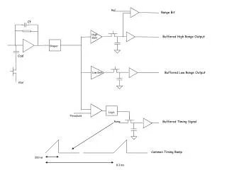
Timing Model Pipeline Functional Model Pipeline Arch State Timing State A functional model for RAMP Gold ParlabManycore • RAMP Gold: A RAMP emulation model for Parlabmanycore • Single-socket tiled manycore target • SPARC v8 -> v9 • Split functional/timing model, both in hardware • Functional model: Executes ISA • Timing model: Capture pipeline timing detail (can be cycle accurate) • Host multithreading of both functional and timing models • Built on BEE3 system • Four Xilinx Virtex 5 LX110T Functional model implementation in this talk
A RAMP Emulator • “RAMP blue” as a proof of concept • 1,008 32-bit RISC core on 105 FPGAs of 21 BEE2 boards • A bigger “RAMP blue” with more FPGAs for Parlab? • Less interesting ISA • High-end FPGAs cost thousands of dollars • CPU cores (@90 MHz) are even slower than memory! • Waste memory bandwidth • High CPI, low pipeline utilization • Poor emulation performance/FPGA • Need a high density and more efficient design
RAMP Gold Implementation • Goal : • Performance : maximize aggregate emulated instruction throughput(GIPS/FPGA) • Scalability: scale with reasonable resource consumption • Design for FPGA fabric • SRAM nature of FPGA: RAMs are cheap! • Efficient for state storage, but expensive for logic (e.g. multiplexer) • Need reconsider some traditional RISC optimizations • By passing network is against “smaller, faster” on FPGAs • ~28% LUT reduction, ~18% frequency improvement on SPARC v8 implementation, wo result forwarding • DSPs are perfect for ALU implementation • Circuit performance limited by routing • Longer pipeline • Carefully mapped FPGA primitives • Emulation latencies: e.g. across FPGAs, memory network • “High” frequency (targeting 150 MHz)
X Y IR PC 1 PC 1 PC 1 PC 1 Host multithreading CPU1 CPU2 CPU63 CPU64 Target Model Functional model on FPGA ALU GPR1 GPR1 I$ DE GPR1 GPR1 D$ +1 Thread Select 6 6 6 • Single hardware pipeline with multiple copies of CPU state • Fine-grained multithreading • Not multithreading target
Pipeline Architecture • Single issue in order pipeline (integer only) • 11pipeline stages (no forwarding) -> 7 logical stages • Static thread scheduling, zero overhead context switch • Avoid complex operations with “microcode” • E.g. traps, ST • Physical implementation • All BRAM/LUTRAM/DSP blocks in double clocked or DDR mode • Extra pipeline stages for routing • ECC/Parity protected BRAMs • Deep submicron effect on FPGAs
Implementation Challenges • CPU state storage • Where? • How large? Does it fit on FPGA? • Minimize FPGA resource consumption • E.g. Mapping ALU to DSPs • Host cache & TLB • Need cache? • Architecture and capacity • Bandwidth requirement and R/W access ports • host multithreading amplifies the requirement
State storage • Complete 32-bit SPARC v8 ISA w. traps/exceptions • All CPU states (integer only) are stored in SRAMs on FPGA • Per context register file -- BRAM • 3register windows stored in BRAM chunks of 64 • 8 (global) + 3*16 (reg window) = 54 • 6 special registers • pc/npc -- LUTRAM • PSR (Processor state register) -- LUTRAM • WIM (Register Window Mask) -- LUTRAM • Y (High 32-bit result for MUL/DIV) -- LUTRAM • TBR (Trap based registers) -- BRAM (packed with regfile) • Buffers for host multithreading (LUTRAM) • Maximum 64 threads per pipeline on Xilinx Virtex5 • Bounded by LUTRAM depth (6-input LUTs)
Mapping SPARC ALU to DSP • Xilinx DSP48E advantage • 48-bit add/sub/logic/mux+ pattern detector • Easy to generate ALU flags: < 10 LUTs for C, O • Pipelined access over 500 MHz
DSP advantage • Instruction coverage (two DSPs / pipeline) • 1 cycle ALU (1 DSP) • LD/ST (address calculation) • Bit-wise logic (and, or, …) • SETHI (value by pass) • JMPL, RETT, CALL (address calculation) • SAVE/RESTORE (add/sub) • WRPSR, RDPSR, RDWIM (XOR op) • Long latency ALU instructions (1 DSP) • Shift/MUL (2 cycles) • 5%~10% logic save for 32-bit data path
Host Cache/TLB • Accelerating emulation performance! • Need separate model for target cache • Per thread cache • Split I/D direct-map write-allocate write-back cache • Block size: 32 bytes (BEE3 DDR2 controller heart beat) • 64-thread configuration: 256B I$, 256B D$ • Size doubled in 32-thread configuration • Non-blocking cache, 64 outstanding requests (max) • Physical tags, indexed by virtual or physical address • $ size < page size • 67% BRAM usage • Per thread TLB • Split I/D direct-map TLB: 8 entries ITLB, 8 entries DTLB • Dummy currently (VA = PA)
Cache-Memory Architecture • Cache controller • Non-blocking pipelinedaccess (3-stages) matches CPU pipeline • Decoupled access/refill: allow pipelined, OOO mem accesses • Tell the pipeline to “replay” inst. on miss • 128-bit refill/write back data path • fill one block in 2 cycles
Example: A distributed memory non-cache coherent system • Eight multithreaded SPARC v8 pipelines in two clusters • Each thread emulates one independent node in target system • 512 nodes/FPGA • Predicted emulation performance: • ~1 GIPS/FPGA (10% I$ miss, 30% D$ miss, 30% LD/ST) • x2 compared to naïve manycore implementation • Memory subsystem • Total memory capacity 16 GB, 32MB/node (512 nodes) • One DDR2 memory controller per cluster • Per FPGA bandwidth: 7.2 GB/s • Memory space is partitioned to emulate distributed memory system • 144-bit wide credit-based memory network • Inter-node communication (under development) • Two-level tree network to provide all-to-all communication
Project Status • Done with RTL implementation • ~7,200 lines synthesizableSystemverilog code • FPGA resource utilization per pipeline on Xilinx V5 LX110T • ~3% logic (LUT), ~10% BRAM • Max 10 pipelines, but back off to 8 or less for timing model • Built RTL verification infrastructure • SPARC v8 certification test suite (donated by SPARC international) + Systemverilog • Can be used to run more programs but very slow • (~0.3 KIPS)
Verification in progress • Tested instructions • All SPARC v7 ALU instructions: add/sub, logic, shift • All integer branch instructions • All special instructions: register window, system registers • Working on: LD/ST and Trap • More verification after P&R and on HW • work with the rest RAMP Gold infrastructure • Lessons so far • Infrastructure is not trivial, and very few sample design available (have to build our own!) • Multithreaded states complicates the verification process! • buffers and shared FU interfaces