Download
1 / 18
180 likes | 298 Views
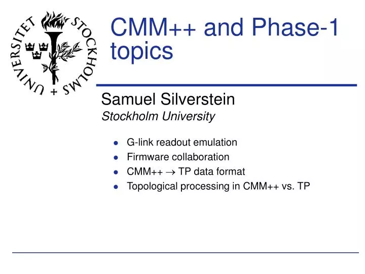
CMM++ and Phase-1 topics. Samuel Silverstein Stockholm University. G-link readout emulation Firmware collaboration CMM++ TP data format Topological processing in CMM++ vs. TP. Current CMM. VME--. VME CPLD. Glink. DAQ and ROI readout. TTCrx. Glink. Input from JEM/CPM.

E N D
CMM++ and Phase-1 topics Samuel Silverstein Stockholm University • G-link readout emulation • Firmware collaboration • CMM++ TP data format • Topological processing in CMM++ vs. TP
Current CMM VME-- VME CPLD Glink DAQ and ROI readout TTCrx Glink Input from JEM/CPM LVDS merger links Virtex E (crate) Virtex E (system) Input from JEM/CPM modules (40 MHz) LVDS outputs to CTP 2
CMM++ concept We want CMM++ to be backward-compatible VME-- Glink DAQ and ROI readout Glink From JEM/CPM SNAP12 Virtex 6 FPGA LVDS merger cables SNAP12 12-fiber bundles SNAP12 SNAP12 Legacy LVDS outputs to CTP SNAP12 4-6 optical Tx and/or Rx modules @ 6.4 Gbit/s From JEM/CPM (160 MHz) SNAP12 3
CMM emulation (first try) VME-- VME CPLD Glink DAQ and ROI readout TTCrx Glink Input from JEM/CPM Implement in Virtex 6 (XC6VHX565T-2FF1924) based on existingJet CMM code LVDS merger links Virtex E (crate) Virtex E (system) Input from JEM/CPM modules (40 MHz) LVDS outputs to CTP Note: no SNAP12 transceivers yet 4
Works, but high I/O use • Available I/O (excluding transceivers):640 pins • Real-time data path: • Backplane input (16 x 25): 400 • Cables (3 x 25): +75 • CTP output (2 x 33): +66 = 541 pins • Control and timing: • VME-- from CPLD 35 • TTC (L1A, BCR, deskew 1 and 2) +4 • Crystal clock +1 • clr_pe,rst,rst_dll,pbk_en,can_mc,en_cblout +6 = 46 pins • Readout: • Glink data outputs 2 x 20 40 • DAV pins 2 = 42 pins • Indicator LEDs : 8 + 8 pins • TOTAL: 637 / 640 (FF1924 package)637 Note: FF1923 package has 720 I/Os (but 8 fewer GTX transceivers)
Emulating Glinks in the FPGA saves about 40 pins VME-- VME CPLD Glink DAQ and ROI readout TTCrx Glink Input from JEM/CPM Readout/Glink block LVDS merger links Virtex E (crate) Virtex E (system) Input from JEM/CPM modules (40 MHz) LVDS outputs to CTP 6
G-link emulation in Virtex 6 DAQ or ROI data word Encodedword G-link encoder 24b 8b multiplexer GTX TX 20b 960 MHz 24b 8b DAV(data available) 40 MHz 40 MHz 120 MHz 120 MHz 7
CMM++ readout block daq_in gdaq 20 DAQ daq_dav daq_reset roi_in groi 20 ROI roi_dav roi_reset daq_locked Clk40 roi_locked Clk120 Easy to drop into top-level design 8
First simulation results non-zero data link lock DAV asserted Reset empty frames sending zeros
There is still work to do... • Implement in ISE, study full timing simulation • Implement on Virtex-6 development board, study timing and jitter • Test with real 9U ROD?
Firmware collaboration • SVN repository • Latest "day-1" jet algo and jet-CMM firmware projects now uploaded to CERN SVN: • https://svnweb.cern.ch/cern/wsvn/atl1calo/firmware/ • Need to do same for upgrade • Full designs (e.g. Jet CMM++) • "Standalone" modules (Glink readout, TP algorithms, etc) • Where? • Also in atl1calo/firmware directory? • Create a separate directory tree or repository? • Reminder: VHDL style guide for L1Calo: • https://edms.cern.ch/file/1100579/0.5/VHDL_guidlines.doc
CMM++ TP data formats Original paradigm: Send full backplane contents immediately to the TP, unprocessed TP From backplane CMM++ ... 16 modules x 24 bits x 160 Mbit/s = 61.44 Gbit/s 12 fibers x 5120 Mbit/s = 61.44 Gbit/s Matched bandwidths 12
Problems with this paradigm • Large total bandwidth to TP • 10 - 12 CMM++ modules 120 - 144 fibers • Not including other possible inputs, for instance muons • Most backplane data will be empty (at least in p-p) • Backplane format accommodates worst-case ROI multiplicity for a CPM/JEM • A single FPGA cannot receive this many links • Must first reduce size of data set before executing "global" algorithms on full event topology • Thus our current quadrant/system paradigm • Can we do better?
Idea: reduce data volume already in the CMM++ • Have each CMM++ produce a zero-suppressed list of ROIs : • Absolute coordinates: 9 bits for jets, 13 bits for clusters • 8 and 11 bits, respectively, if crate number implicit • Thresholds: 8 bits per ROI • Additional information (energy, etc): 10-12 bits per ROI • Total: ~31 bits per ROI • One 6.4 Gbit/s fiber has a 128-bit data payload per BC • Up to four ROIs per fiber per BC • 4 fibers 16 ROIs / CMM++ (3 data reduction) • 6 fibers 24 ROIs / CMM++ (2 data reduction) • Use bit 32 to signal "last ROI" • Lets us know if max number of ROIs was exceeded
With 6 fibers per CMM++, one FPGA can receive all L1Calo data Example: CMM++ only solution (TP also simplified) EM Energy Jet EM EM/ EM/ CP1 C M M + + C M M + + C M M + + JEP0 C M M + + C M M + + CP0 C M M + + CLUSTER JET ENERGY LVDS C M M + + CP3 C M M + + C M M + + JEP1 (TP) C M M + + CP2 C M M + + C M M + + ~56 L1Calo fibers to "TP" (48 CP + 6 Jet + 2 Energy)
TP implementation • Two baseline options: • Designated CMM++ in system • Topological processor (TP) crate • TP crate is the preferred choice • Scalable: several FPGAs could perform algorithms in parallel • Room for more inputs (e.g. muons) • Prepares us better for Phase II • But should keep CMM++ option open • If TP is delayed, for instance
Implications of CMM++ option • Algorithm limitations • If all L1Calo ROIs available, can probably perform any L1Calo-only algorithm • But only one FPGA, so we don't have unlimited resources to perform many algorithms • Latency • Probably no significant difference
Implications of CMM++ option • Readout • Probably will read out TP to 9U RODs (Glink) • TP-CMM must read out crate-level CMM++ I/O plus TP inputs/outputs • Need two sets of G-link readout ports on CMM++ • Readout FIFOs • 160 MHz backplane format gives 1600 bits/BC, plus cables and outputs, to be pipelined for CMM++ readout • TP will also have many bits of input data to be pipelined and read out. • So a combined CMM++ and TP FPGA might need to use a lot of its memory resources just for readout. • Add external pipeline memories?