Download
1 / 23
230 likes | 271 Views
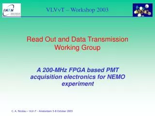
Explore the design and components of the innovative FPGA-based PMT acquisition electronics for the NEMO Km3 experiment, including tower configurations, junction boxes, data rates, and self-calibration processes.

E N D
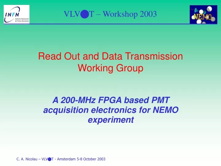
Read Out and Data TransmissionWorking Group • A 200-MHz FPGA based PMT acquisition electronics for NEMO experiment
The NEMO Km3 experiment 200 m Tower 200 m Secondary JB 1400 m Primary JB Main electro optical cable 64 towers placed on a square grid (8x8). The towers are electro-optically linked (8 by 8) to one of the 8 so called secondary junction boxes (S-JB). The S-JBs are then connected to the so called primary junction box (P-JB) which links the apparatus to the main electro-optical cable arriving from on shore.
The Tower 19.44 Mbps STM-1 (155 Mbps) Data On Fiber 2.5 Gbps FCM (Floor Control Module) Benthosphere DAQ Tower Junction-Box (Optical Interleaver) Secondary Junction-Box
Data acquisition electronics benthosphere PSU DAQ Board Three twisted pairs PMT Floor Control Module
Constraints PMT Signal: Bandwidth 100MHz Output voltage range: 0 -40V Threshold value for L0 trigger: ~ -30mV (~1/4 photoelectron for 13’’ PMT) Single photoelectron rate (due to 40K ): Event rate (with a 13” PMT): ~50 kevents/s Event length: ~50ns Electro-mechanical: Power consumption as low as possible (long distance power transport). Long mean time between failure (no repairing possible). Small & simple (the fewer the components the more reliable the system).
Constraints: consequences PMT SignalBandwidth: 100MHz Sampling rate: 200MHz PMT Signal Dynamics:-40V / -30mV ~ 1300 2048 (11 bit) Sampling resolution: 8 bit Quasi logarithmic analog compression DAQInput Signal Dynamics:-40V / -18mV Physical data rate(for a 13” PMT): 50 kevents/s X (100 bit/event) ~ 5Mbps Sampling data rate: 200MHz X 8bit = 1.6Gbps Thus, using a user definable digital threshold, the sampling data rate can be reduced to the expected value of 5Mbps.
Block diagram 8 Digital I/O lines AFE 200Msps ADC MOD/DEM + POWER PMT FPGA Clock in Pt Temp.Sens. Analog I/O (7 in, 4 out) 12 bit DAC Data/Control out 8 ch Flash EPROM DSP 10 bit ADC 8 ch ssi Power + Control PTS AFE JTAG RS232
The Analog Front End Analog Front End - Impedence matching ( 50 Ohm ) - Passive quasi-logarithmic signal compression - The compression is obtained using a diode, the charachteristic of which varies mainly with temperature, which can be measured through a platinum temperature sensor. - Since modelling of the characteristic curve of the diode is difficult, the system self-measures the compression curve allowing onshore data decompression (self calibration). 8 Digital I/O lines AFE 200Msps ADC MOD/DEM + POWER PMT FPGA Clock in Pt Temp.Sens. Analog I/O (7 in, 4 out) 12 bit DAC Data/Control out 8 ch Flash EPROM DSP 10 bit ADC 8 ch ssi Power + Control PTS AFE Two 12-bit-DACs are used to perform the self-calibration. JTAG RS232
The Analog Front End 8 Digital I/O lines Analog Front End: compressor schematic - only passive components. - it’s possible, by changing the resistor’s value, to change the compression curve. AFE 200Msps ADC MOD/DEM + POWER PMT FPGA Clock in Pt Temp.Sens. 470 38 20 12 470 470 Analog I/O (7 in, 4 out) 12 bit DAC Data/Control out 8 ch Flash DSP 10 bit ADC 8 ch ssi Power + Control PTS AFE JTAG RS232
The Analog Front End: calibration curve 0 512 1024
200 Msample/s analog to digital conversion 8 Digital I/O lines AFE 200Msps ADC MOD/DEM + POWER PMT FPGA The 200Msps ADC To reduce power consumption two 100MHz 8-bit differential FlashADCs are used. One is triggered on the 100MHz clk signal. The other is triggered on the NOT(clk) signal. Clock in Pt Temp.Sens. Analog I/O (7 in, 4 out) 12 bit DAC Data/Control out 8 ch Flash DSP 10 bit ADC 8 ch ssi Power + Control PTS AFE Two 12-bit-DACs are used to set the proper offset. JTAG RS232
The Auxiliary analog I/Os 8 Digital I/O lines AFE 200Msps ADC MOD/DEM + POWER PMT FPGA Clock in Pt Temp.Sens. Analog I/O (7 in, 4 out) 12 bit DAC Data/Control out 8 ch Flash DSP 10 bit ADC 8 ch ssi Power + Control PTS AFE JTAG RS232 The auxiliary analog Inputs: 8-channel 10-bit-ADC - one channel is used for measuring the temperature of the compressor diode. - the other 7 channels are led to an external connector
The Auxiliary analog I/Os 8 Digital I/O lines AFE 200Msps ADC MOD/DEM + POWER PMT FPGA Clock in Pt Temp.Sens. Analog I/O (7 in, 4 out) 12 bit DAC Data/Control out 8 ch Flash DSP 10 bit ADC 8 ch ssi Power + Control PTS AFE JTAG RS232 The auxiliary analog Outputs: 8 channel 12 bit DAC - 2 channels are used for self-calibration - 2 channels are used for adjusting the offset of the two 100 Msps differential ADCs. - other 4 channels are led to an external connector
The DSP 8 Digital I/O lines AFE 200Msps ADC MOD/DEM + POWER PMT FPGA Clock in Pt Temp.Sens. Analog I/O (7 in, 4 out) 12 bit DAC Data/Control out 8 ch Flash DSP 10 bit ADC 8 ch ssi Power + Control PTS AFE JTAG RS232 The DSP: - wake-up (reads the flash memory) - loads the FPGA bitstream - controls the threshold settings - generates the 100MHz clock (PLL) - controls the auxiliary analog I/O (offset, self-calibration) via SSI - JTAG (debug) - RS232 (for debug and/or instrumentation control)
The MOD/DEM block 8 Digital I/O lines AFE 200Msps ADC MOD/DEM + POWER PMT FPGA Clock in Pt Temp.Sens. Analog I/O (7 in, 4 out) 12 bit DAC Data/Control out 8 ch Flash EPROM DSP 10 bit ADC 8 ch ssi Power + Control PTS AFE JTAG RS232 • The MOD/DEM: • Connects the Board to the host • receives Clock signal (1.215 MHz) • receives control signals • (45 * 9.6kbps = 432 kbps) • sends data and control signals (19.44 Mbps) • receives power (5 VDC) • All connections are electric (3 twisted pairs).
The FPGA 8 Digital I/O lines AFE 200Msps ADC MOD/DEM + POWER PMT FPGA Clock in Pt Temp.Sens. Analog I/O (7 in, 4 out) 12 bit DAC Data/Control out 8 ch Flash EPROM DSP 10 bit ADC 8 ch ssi Power + Control PTS AFE JTAG RS232 The FPGA: connections: - 200 MBps from the fast ADCs - ~1MBps to/from the DSP - 19.44 Mbps to the MOD/DEM - 432 kbps from the MOD/DEM
Inside the FPGA:block diagram 8 Digital I/O lines Data out Data (PMT + Slow Control) ADC FIFO Data from PMT Packet formatter SOC MOD/DEM ADC Slow Control Data PMT cal SOC time calibration & command parser Prog. trigger Slow Control & Timing Time Register TR Reset Slow Control Commands 1.215MHz decoder 1.215MHz Clock 97.2 MHz DSP Bus FPGA To DSP PLL From DSP PLL DSP
Inside the FPGA:The 100Mhz clock generation 8 Digital I/O lines Data out Data (PMT + Slow Control) ADC FIFO Data from PMT Packet formatter SOC MOD/DEM ADC Slow Control Data PMT cal SOC time calibration & command parser Prog. trigger Slow Control & Timing Time Register TR Reset Slow Control Commands 1.215MHz decoder 1.215MHz Clock 97.2 MHz DSP Bus FPGA To DSP PLL From DSP PLL - 1.215 MHz is generated by the FCM (19.44MHz / 16) - 97.2 MHz square wave is obtained from the DSP PLL (1.215 * 80) - the sampling frequency is obtained using both (rising & falling) edges of the 97.2MHz square wave clock signal. DSP
Inside the FPGA:The FIFO and the threshold 8 Digital I/O lines Data out Data (PMT + Slow Control) ADC FIFO Data from PMT Packet formatter SOC MOD/DEM ADC Slow Control Data PMT cal SOC time calibration & command parser Prog. trigger Slow Control & Timing Time Register TR Reset Slow Control Commands 1.215MHz decoder 1.215MHz Clock 97.2 MHz DSP Bus FPGA To DSP PLL From DSP PLL - the threshold value for the L0 trigger can be changed at runtime by the user. - some pretrigger samples are stored in the FIFO as well as the timestamp of the threshold time DSP
Inside the FPGA:The packet parser/formatter 8 Digital I/O lines Data out Data (PMT + Slow Control) ADC FIFO Data from PMT Packet formatter SOC MOD/DEM ADC Slow Control Data PMT cal SOC time calibration & command parser Prog. trigger Slow Control & Timing Time Register TR Reset Slow Control Commands 1.215MHz decoder 1.215MHz Clock 97.2 MHz DSP Bus FPGA To DSP PLL From DSP PLL - collects data from the FIFO (PMT data) and data from the DSP (slow control data) - creates the bitstream to be sent to the FCM DSP
Inside the FPGA:The packet parser/formatter 8 Digital I/O lines Data out Data (PMT + Slow Control) ADC FIFO Data from PMT Packet formatter SOC MOD/DEM ADC Slow Control Data PMT cal SOC time calibration & command parser Prog. trigger Slow Control & Timing Time Register TR Reset Slow Control Commands 1.215MHz decoder 1.215MHz Clock 97.2 MHz DSP Bus FPGA To DSP PLL From DSP PLL - It’s fed with the slow control data stream. - It “recognizes” and executes the time calibration commands. These commands have to be executed by hardware (to be software delay free). For example: for the measurement of the PMT latency time a LED can be controlled by one of the 8 digital I/O. - Other commands are directly sent to the DSP. DSP
The protoype Characteristics: FPGA: Xilinx XC4028XLA DSP: Motorola DSP56303 100Msps ADCs: AD9283 Physical dimensions: 2 x (10 cm) x (10 cm) Power consumption: ~950mW DAQ MOD/DEM + HVPSU
Flexibility towards the Km3 - The allocated bandwidth of the output data channel is over-dimensioned compared to the physical one. Thus, by changing the FPGA firmware, it’s possible to allocate different data bandwidth. - The number of auxiliary channels is reduntant. Probably, for the NEMO Km3 we won’t need all the 7 A/D channels, 4 D/A channels, 8 digital I/O lines, reducing number of components, power consumption, and physical dimension. - Using newer FPGA, it’s possible to implement the DSP functions inside the FPGA, reducing dimensions, power consumption, costs. Goal: power consumption < 500mW