Download
1 / 1
20 likes | 138 Views
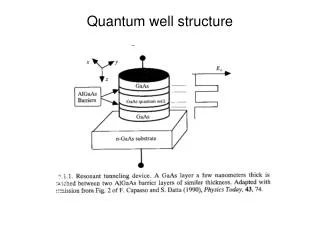
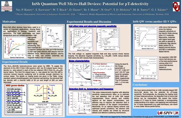
InSb Quantum Well Micro-Hall Devices: Potential for pT-detectivity. 3. AlP. AlAs. GaP. 2. AlSb. Vas. P. Kunets a) , S. Easwaran a) , W. T. Black a) , D. Guzun a) , Yu. I. Mazur a) , N. Goel b) , T. D. Mishima b ) , M. B. Santos b) , G. J. Salamo a). GaAs. Energy Bandgap (eV). InP. 1.

E N D
InSb Quantum Well Micro-Hall Devices: Potential for pT-detectivity 3 AlP AlAs GaP 2 AlSb Vas. P. Kunetsa), S. Easwarana), W. T. Blacka), D. Guzuna), Yu. I. Mazura), N. Goelb), T. D. Mishimab), M. B. Santosb), G. J. Salamoa) GaAs Energy Bandgap (eV) InP 1 GaSb InSb InAs a) Physics Department, University of Arkansas, Fayetteville, USA; b) Homer L. Dodge Department of Physics and Astronomy, University of Oklahoma, Norman, USA 0 5.5 6.0 6.5 Lattice Constant (Å) Fit of Noise Spectrum: • Fitting Parameters: • - Hooge parameter Ai– amplitude of G-R noise i– time constant for G-R Hooge Law: d-doping d-doping MBE grown device We have demonstrated that an InSb remotely-doped QW micro-Hall device has the potential for pT-range sensitivity. Technologically, by changing the doping level of these heterostructures, the detection limit of micro-Hall device can be manipulated. We expect that further studies of 1/f noise for these materials, a corresponding understanding of its origins, and applying new techniques for 1/f noise suppression (e.g. gate technique), can result in even better device performance. E3 30 Å InSb cap layer 97 Å Al0.12In0.88Sb E2 1 EF 970 Å Al0.12In0.88Sb 2 Al0.12In0.88Sb Al0.12In0.88Sb 390 Å Al0.12In0.88Sb E1 250 Å InSb QW 390 Å Al0.12In0.88Sb InSb QW 2 2 m Al0.12In0.88Sb 0.2 m Al0.24In0.76Sb 1 m Al0.12In0.88Sb 1 m AlSb GaAs (001) substrate InSb QW versus another III-V QWs Motivation Experimental Results and Discussion Hall effect data and absolute magnetic sensitivity InSb micro-Hall devices show the highest magnetic sensitivity at low electric fields among other III-V materials. Meanwhile, materials with higher band gap are able to operate at sufficiently high electric fields (where DC is doped-channel device and MD is modulation-doped device. Micro-Hall effect devices have been used in a variety of important applications. Among these are applications in biology, medicine and spintronics. The main advantages are room temperature and non-contact operation, high high spatial resolution, portability and digital signal processing. The best materials for a magnetic sensors are InAs and InSb because of their high peak electron drift velocity and low effective mass. Micron-sized devices utilizing InAs or InSb, can resolve extremely low magnetic fields in the nT-range. The Hall voltage vs. applied magnetic field and bias current shows device linearity. The absolute magnetic sensitivity, SA = dVH/dB = GvW, versus electric field tracks the drift velocity-field characteristics. As expected, InSb QW micro-Hall devices are of the best performance among other III-V micro-Hall devices based on heterostructures. Experimental Details Noise characteristics Using the best fit, the Hooge parameter of 2.710-3, 2.6810-3 and 1.3410-3 was found for samples S944, S945 and S946, respectively. The G-R process with 2 ms was revealed. The AlxIn1-xSb/InSb heterostructures were grown by MBE. To supply the electrons to the 250 Å thick InSb quantum well, two Si--doped layers (same density 2) were placed in each of the two adjacent 390 Å thick Al0.12In0.88Sb barrier layers. The third Si--doped layer, 1, was placed far from the well to minimize ionized impurity scattering and to provide enough electrons for surface states. The details on doping levels are given in the Table. Using standard optical photolithography and chemical wet-etching, five-terminal Hall bar devices with a channel width of 35 m and length of 200 m were fabricated. Conclusions Detection limit vs. temperature and frequency The noise measurements together with absolute sensitivity measurements allow us to estimate the real detection limit of InSb QW based magnetometer. Since velocity and mobility depend on the dopant concentration, one effective way to improve the detection limit is through variation of the dopant concentration. Meanwhile, for an optimal doping scheme and optimized growth conditions, the electron drift velocity and mobility are limited by structural defects and effective scattering mechanisms. This work was supported by National Science Foundation through grants DMR-0510056 amd DMR-0520550