Download
1 / 28
290 likes | 405 Views
Explore the concepts of PN junctions, thermal equilibrium, and MOS capacitors. Learn about charge storage, reverse bias effects, and voltage dependence. Dive into capacitance variations and practical applications in radio tuners and transmission lines.

E N D
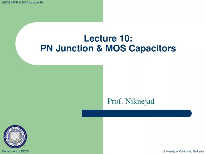
Lecture 10: PN Junction & MOS Capacitors Prof. Niknejad
Lecture Outline • Review: PN Junctions Thermal Equilibrium • PN Junctions with Reverse Bias (3.3-3.6) • MOS Capacitors (3.7-3.9): • Accumulation, Depletion, Inversion • Threshold Voltage • CV Curve University of California, Berkeley
Results of MT #1 • Good Job! • This is only 17% of your grade Homework 15% Laboratory 20% Midterm #1 17% Midterm #2 18% Final 30% University of California, Berkeley
PN Junction in Thermal Equilibrium • Contact potential develops between P and N region • Diffusion current balanced by drift current • Depletion region is a “space-charge” region where the concentration of free carriers is low • The depletion region is charged due to the immobile background ions (donors and acceptors) • Used the “Depletion Approximation” to estimate the charge density calculate the electric fields and potential variation using electrostatics in 1D University of California, Berkeley
? Have we invented a battery? • Can we harness the PN junction and turn it into a battery? • Numerical example: University of California, Berkeley
+ − n p Contact Potential • The contact between a PN junction creates a potential difference • Likewise, the contact between two dissimilar metals creates a potential difference (proportional to the difference between the work functions) • When a metal semiconductor junction is formed, a contact potential forms as well • If we short a PN junction, the sum of the voltages around the loop must be zero: University of California, Berkeley
PN Junction Capacitor • Under thermal equilibrium, the PN junction does not draw any current • But notice that a PN junction stores charge in the space charge region (transition region) • Since the device is storing charge, it’s acting like a capacitor • Positive charge is stored in the n-region, and negative charge is in the p-region: University of California, Berkeley
+ − Reverse Biased PN Junction • What happens if we “reverse-bias” the PN junction? • Since no current is flowing, the entire reverse biased potential is dropped across the transition region • To accommodate the extra potential, the charge in these regions must increase • If no current is flowing, the only way for the charge to increase is to grow (shrink) the depletion regions University of California, Berkeley
+ − Current Under Reverse Bias • Under thermal equilibrium current is zero • If we apply a reverse bias, we are increasing the barrier against diffusion current • Drift current is low since the field only moves minority carriers across junction • In fact, current is not zero but very small since the minority carrier concentration is low. Minority carriers within one diffusion length of junction can contribute to a reverse bias current. This is more or less independent of the applied bias n p University of California, Berkeley
Voltage Dependence of Depletion Width • Can redo the math but in the end we realize that the equations are the same except we replace the built-in potential with the effective reverse bias: University of California, Berkeley
Charge Versus Bias • As we increase the reverse bias, the depletion region grows to accommodate more charge • Charge is not a linear function of voltage • This is a non-linear capacitor • We can define a small signal capacitance for small signals by breaking up the charge into two terms University of California, Berkeley
Derivation of Small Signal Capacitance • From last lecture we found • Notice that University of California, Berkeley
Physical Interpretation of Depletion Cap • Notice that the expression on the right-hand-side is just the depletion width in thermal equilibrium • This looks like a parallel plate capacitor! University of California, Berkeley
A Variable Capacitor (Varactor) • Capacitance varies versus bias: • Application: Radio Tuner University of California, Berkeley
Oxide N-type Diffusion Region P-type Si Substrate “Diffusion” Resistor • Resistor is capacitively isolation from substrate • Must Reverse Bias PN Junction! • PN Junction creates a distributed capacitance with substrate (RC transmission line) University of California, Berkeley
Gate (n+ poly) Body (p-type substrate) MOS Capacitor • MOS = Metal Oxide Silicon • Sandwich of conductors separated by an insulator • “Metal” is more commonly a heavily doped polysilicon layer n+ or p+ layer • NMOS p-type substrate, PMOS n-type substrate Oxide (SiO2) Very Thin! University of California, Berkeley
Gate (n+ poly) Body (p-type substrate) P-I-N Junction • Under thermal equilibrium, the n-type poly gate is at a higher potential than the p-type substrate • No current can flow because of the insulator but this potential difference is accompanied with an electric field • Fields terminate on charge! University of California, Berkeley
+ − + − Body (p-type substrate) − − − − − − − − − − − − − − − − − − − − − − − − − − Fields and Charge at Equilibrium • At equilibrium there is an electric field from the gate to the body. The charges on the gate are positive. The negative charges in the body come from a depletion region ++++++++++++++++++ University of California, Berkeley
Body (p-type substrate) + − Good Place to Sleep: Flat Band • If we apply a bias, we can compensate for this built-in potential • In this case the charge on the gate goes to zero and the depletion region disappears • In solid-state physics lingo, the energy bands are “flat” under this condition University of California, Berkeley
− + Body (p-type substrate) Accumulation • If we further decrease the potential beyond the “flat-band” condition, we essentially have a parallel plate capacitor • Plenty of holes and electrons are available to charge up the plates • Negative bias attracts holes under gate −−−−−−−−−−−−−−−−−− ++++++++++++++++++ University of California, Berkeley
− − − − − − − − − Body (p-type substrate) − − − − − − − − + − Depletion • Similar to equilibrium, the potential in the gate is higher than the body • Body charge is made up of the depletion region ions • Potential drop across the body and depletion region + + + + + + + + + + University of California, Berkeley
− − − − − − − − − Body (p-type substrate) − − − − − − − − + − Inversion • As we further increase the gate voltage, eventually the surface potential increases to a point where the electron density at the surface equals the background ion density • At this point, the depletion region stops growing and the extra charge is provided by the inversion charge at surface + + + + + + + + + + University of California, Berkeley
Threshold Voltage • The threshold voltage is defined as the gate-body voltage that causes the surface to change from p-type to n-type • For this condition, the surface potential has to equal the negative of the p-type potential • We’ll derive that this voltage is equal to: University of California, Berkeley
Inversion Stops Depletion • A simple approximation is to assume that once inversion happens, the depletion region stops growing • This is a good assumption since the inversion charge is an exponential function of the surface potential • Under this condition: University of California, Berkeley
Q-V Curve for MOS Capacitor • In accumulation, the charge is simply proportional to the applies gate-body bias • In inversion, the same is true • In depletion, the charge grows slower since the voltage is applied over a depletion region inversion depletion accumulation University of California, Berkeley
Numerical Example • MOS Capacitor with p-type substrate: • Calculate flat-band: • Calculate threshold voltage: University of California, Berkeley
Num Example: Electric Field in Oxide • Apply a gate-to-body voltage: • Device is in accumulation • The entire voltage drop is across the oxide: • The charge in the substrate (body) consist of holes: University of California, Berkeley
Numerical Example: Depletion Region • In inversion, what’s the depletion region width and charge? University of California, Berkeley