Download
1 / 33
350 likes | 636 Views
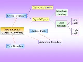
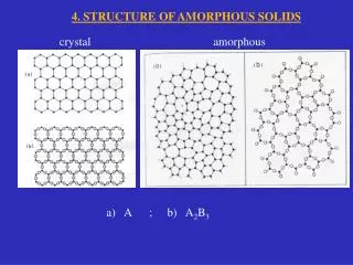
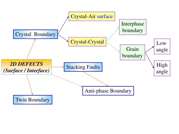
2D DEFECTS (Surface / Interface). Anti-phase Boundary. Crystal-Air surface. Interphase boundary. Crystal Boundary. Crystal-Crystal. Low angle. Grain boundary. High angle. Stacking Faults. Twin Boundary. Low angle. High angle. Based on angle of rotation. Twist. Homophase. Tilt.

E N D
2D DEFECTS(Surface / Interface) Anti-phase Boundary Crystal-Air surface Interphaseboundary Crystal Boundary Crystal-Crystal Low angle Grainboundary Highangle Stacking Faults Twin Boundary
Low angle High angle Based on angle of rotation Twist Homophase Tilt Based on axis Mixed Based on Lattice Models Special CSL/Other Random Based on Geometryof the Boundary plane Curved Faceted Mixed
Curtesy S. Van Tenderloo Picture ARM-UC Berkeley4
Low angle Semicoherent High angle Incoherent Based on angle of rotation Twist Interphase Tilt Based on axis Mixed Based on Lattice Models Special Epitaxial/Coherent Random Based on Geometryof the Boundary plane Curved Wulff-type constructions Faceted Mixed
Coherence at interfaces • Coherent interface means an interface in which the atoms match up on a 1-to-1 basis (even if some elastic strain is present). • Incoherent interface means an interface in which the atomic structure is disordered. • Semi-coherent interface means an interface in which the atoms match up, but only on a local basis, with defects (dislocations) in between.
Coherent interfaces • Coherent interface means an interface in which the atoms match up on a 1-to-1 basis (even if some elastic strain is present). • Near identical lattice parameters, often thin layers of A on B
Incoherent interfaces • Incoherent interface means an interface in which the atomic structure is disordered. • General case, analogous to a general high-angle grain boundary (roughly)
Semi-coherent interfaces • Semi-coherent interface means an interface in which the atoms match up, but only on a local basis, with defects (dislocations) in between. • Comparable to a low-angle grain boundary with a dislocation array (now called misfit dislocations)
Epitaxy Britannica Concise Encyclopedia:epitaxy Process of growing a crystal of a particular orientation on top of another crystal. If both crystals are of the same material, the process is known as homoepitaxy; if the materials are different, it is known as heteroepitaxy. Common types of epitaxy include vapour phase, liquid phase, and solid phase, according to the source of the atoms being arranged on the substrate. Comment 1: “growth” is not needed here… Comment 2: often used more generally than this
Main Types of Epitaxy • Homoepitaxy • Growth of material on the same substrate (Si on Si) • Pseudomorphic growth • Material adopts the lattice of substrate/matrix • Coincidence • Material has certain spacings common with substrate/matrix • Similar to CSL • Cube-Cube • Major orientations are parallel, e.g. [001]A//[001] substrate
Volmer-Weber Frank-van der Merwe Stranski-Krastanov 2 1 layer-by-layer trade surface for interface relieve stress Heteroepitaxial growth modes
Pseudomorphic Growth • Consider a layer of “A” on “B”, of thickness t • Take z normal to film, x in plane • Suppose that lattice of A is larger than that of B, and would match that of B is strained by exx along x • Strain energy scales as texx2 (I leave to you to work this out in detail…) per unit area
Interface Energy • If A matches the lattice of B, the “bonding” will be good • Energy of interface per unit area is gAB • Total energy of system • E = t*exx2 + gAB
Alternative • Hetero epitaxial growth (“lattice-mismatched” growth) permits the fabrication of dissimilar materials on the same substrate • Strain in the growing film depends on thickness and mismatch Thin layer- the film will elastically deform to match the in-plane lattice parameter of the substrate Thick layer- film will revert to its unstrained lattice parameter, with misfit dislocations at the interface with the substrate
Alternative, dislocations • Put dislocations at the interfaces of Burgers vector b, separation L • Assume that these remove all the strain • b/L = exx • Energy of dislocations per unit area will scale as b2/L (better, use Read-Shockley model or similar, Frank-Van Der Merwe) • Note: no t dependence T T T T
Energy Balance • For “phase transition” pseudomorphic to dislocations DE = -C1*t*exx2 + C2(b2/L)
T T T T m1 > m2 T T T T m1 < m2 Dislocation Standoff Dislocation energy scales with shear modulus m1 T T T T m2 m1 = m2
Energy Balance • Better, consider a half dislocation loop growing in (kinetics) • Energy of loop = pRC2b2 • Strain energy relieved = C1pR2/2exx2 • For transition (remove p & 1/2) DE = -C1R2exx2 + RC2b2 R
B1-AlN VN 3 nm Figure 3 Similar Cases • Thin films/precipitates can have different structures • Energy for phase change < interface energy DE = C1*V + C2V2/3(gA-gB)
Al N w-AlN zb-AlN B1-AlN Epitaxial Stabilization of B1-AlN in AlN/VN Superlattices aVN Energy of B1-AlN and zb-AlN vs. underlayer lattice constant (not including the interfacial energy). [Madan et al.]
Similar Cases • Nanoparticles can have different structures • Energy for elastic strain < surface energy DE = C1*V + (CA-CB)V2/3gA
Stranski-Krastanow Growth • Formation of 3D structures (q-dots) preceded by wetting layer • Relieve strain energy, increase surface energy DE = C1V2/3+C2V
Comments • Similar to CSL boundaries, one can have dislocations of the coherency between the two materials at an interface • A step at the interface is normally a different type of dislocation – sessile (immobile) • There is more….
Low angle Semicoherent High angle Incoherent Based on angle of rotation Twist Interphase Tilt Based on axis Mixed Based on Lattice Models Special Epitaxial/Coherent Random Based on Geometryof the Boundary plane Curved Wulff-type constructions Faceted Mixed
Curtesy S. Van Tenderloo Picture ARM-UC Berkeley30