Download
1 / 46
930 likes | 2.08k Views
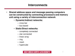
VLSI Interconnects. Instructed by Shmuel Wimer Eng. School, Bar-Ilan University Credits: David Harris Harvey Mudd College (Some material copied/taken/adapted from Harris’ lecture notes). Outline. Introduction Wire Resistance Wire Capacitance Wire RC Delay Crosstalk Wire Engineering

E N D
VLSI Interconnects Instructed by Shmuel Wimer Eng. School, Bar-Ilan University Credits: David Harris Harvey Mudd College (Some material copied/taken/adapted from Harris’ lecture notes) VLSI Interconnects
Outline • Introduction • Wire Resistance • Wire Capacitance • Wire RC Delay • Crosstalk • Wire Engineering • Repeaters • Scaling VLSI Interconnects
Introduction • Chips are mostly made of wires called interconnect • Alternating layers run orthogonally VLSI Interconnects
Transistors are little things under the wires • Many layers of wires VLSI Interconnects
Wires are as important as transistors • Speed • Power • Noise VLSI Interconnects
w s l t h Wire Geometry • Pitch = w + s • Aspect ratio: AR = t/w • Old processes had AR << 1 • Modern processes have AR 2 • Pack in many skinny wires VLSI Interconnects
Layer T (nm) (nm) (nm) W S AR 6 1720 860 860 2 . 0 5 1600 800 800 2 . 0 4 1080 540 540 2 . 0 3 700 320 320 2 . 2 2 700 320 320 2 . 2 Layer Stack • Modern processes use 6-10+ metal layers • Example: Intel 180 nm process • M1: thin, narrow (< 3l) • High density cells • M2-M4: thicker • For longer wires • M5-M6: thickest • For VDD, GND, clk Substrate 1 480 250 250 1 . 9 VLSI Interconnects
w w l w l l t t 4 Rectangular Blocks 1 Rectangular Block R = R (2L/2W) W R = R (L/W) W = R (L/W) W Wire Resistance • r = resistivity (W*m) • R = sheet resistance (W/) • is a dimensionless unit(!) • Count number of squares • R = R * (# of squares) VLSI Interconnects
Choice of Metals • Until 180 nm generation, most wires were aluminum • Modern processes use copper • Cu atoms diffuse into silicon and damage FETs • Must be surrounded by a diffusion barrier VLSI Interconnects
Sheet Resistance • Typical sheet resistances in 180 nm process VLSI Interconnects
Contacts Resistance • Contacts and vias also have 2-20 W • Use many contacts for lower R • Many small contacts for current crowding around periphery VLSI Interconnects
s w layer n+1 C h top 2 t layer n C C adj h bot 1 layer n-1 Wire Capacitance • Wire has capacitance per unit length • To neighbors • To layers above and below • Ctotal = Ctop + Cbot + 2Cadj VLSI Interconnects
Capacitance Trends • Parallel plate equation: C = eA/d • Wires are not parallel plates, but obey trends • Increasing area (W, t) increases capacitance • Increasing distance (s, h) decreases capacitance • Dielectric constant • e = ke0 • e0 = 8.85 x 10⁻¹⁴ F/cm • k = 3.9 for SiO2 • Processes are starting to use low-k dielectrics • k 3 (or less) as dielectrics use air pockets VLSI Interconnects
m) m (aF/ total C M2 Capacitance Data • Typical wires have ~ 0.2 fF/mm • Compare to 2 fF/mm for gate capacitance 400 • Capacitance increases with metal planes above and below • Capacitance decreases with spacing 350 300 M1, M3 planes s = 320 250 s = 480 s = 640 8 s= 200 Isolated s = 320 150 s = 480 s = 640 100 8 s= 50 0 0 500 1000 1500 2000 w (nm) VLSI Interconnects
Diffusion & Polysilicon • Diffusion capacitance is very high (about 2 fF/mm) • Comparable to gate capacitance • Diffusion also has high resistance • Avoid using diffusion (and polysilicon) runners for wires! • Polysilicon has lower C but high R • Use for transistor gates • Occasionally for very short wires between gates VLSI Interconnects
N segments R R/N R/N R/N R/N C C/N C/N C/N C/N R R/2 R/2 R C/2 C/2 C C p L-model -model T-model Lumped Element Models • Wires are a distributed system • Approximate with lumped element models • 3-segment p-model is accurate to 3% in simulation VLSI Interconnects
W W W 260 260 260 167 fF 167 fF 167 fF 167 fF 167 fF 167 fF RC Example • Metal2 wire in 180 nm process • 5 mm long • 0.32 mm wide • Construct a 3-segment p-model • R = 0.05 W/ => R = 781 W • Cpermicron = 0.2 fF/mm => C = 1 pF VLSI Interconnects
W 781 500 fF W 500 fF 4 fF 690 Driver Wire Load Wire RC Delay Example • Estimate the delay of a 10x inverter driving a 2x inverter at the end of the 5mm wire from the previous example • R = 2.5 kW*mm for gates • Unit inverter: 0.36 mm nMOS, 0.72 mm pMOS • tpd = 1.1 ns VLSI Interconnects
Crosstalk • A capacitor does not like to change its voltage instantaneously • A wire has high capacitance to its neighbor. • When the neighbor switches from 1→ 0 or 0→ 1, the wire tends to switch too. • Called capacitive coupling or crosstalk • Crosstalk effects • Noise on non switching wires • Increased delay on switching wires VLSI Interconnects
A B C C C adj gnd gnd Miller Effect • Assume layers above and below on average are quiet • Second terminal of capacitor can be ignored • Model as Cgnd = Ctop + Cbot • Effective Cadj depends on behavior of neighbors • Miller effect Delay and power increase VLSI Interconnects
Aggressor D V aggressor C adj Victim D C V gnd-v victim Crosstalk Noise • Crosstalk causes noise on non switching wires • If victim is floating: • model as capacitive voltage divider VLSI Interconnects
R Aggressor aggressor C D V gnd-a aggressor C adj R Victim victim D C V gnd-v victim Driven Victims • Usually victim is driven by a gate that fights noise • Noise depends on relative resistances • Victim driver is in linear region, agg. in saturation • If sizes are same, Raggressor = 2-4 x Rvictim VLSI Interconnects
Coupling Waveforms • Simulated coupling for Cadj = Cvictim Aggressor 1.8 1.5 1.2 Victim (undriven): 50% 0.9 0.6 Victim (half size driver): 16% Victim (equal size driver): 8% 0.3 Victim (double size driver): 4% 0 0 200 400 600 800 1000 1200 1400 1800 2000 t (ps) VLSI Interconnects
Noise Implications • So what if we have noise? • If the noise is less than the noise margin, nothing happens • Static CMOS logic will eventually settle to correct output even if disturbed by large noise spikes • But glitches cause extra delay • Also cause extra power from false transitions • Dynamic logic never recovers from glitches • Memories and other sensitive circuits also can produce the wrong answer VLSI Interconnects
Wire Engineering VLSI Interconnects
Goal: achieve delay, area, power goals with acceptable noise • Degrees of freedom: • Width • Spacing • Layer • Shielding a vdd a a gnd a a vdd vdd a gnd vdd a gnd a b a b a b 1 0 1 2 3 0 2 0 0 1 1 2 2 VLSI Interconnects
Wire Length: l Driver Receiver N Segments Segment l/N l/N l/N Driver Repeater Repeater Repeater Receiver Repeaters • R and C are proportional to l • RC delay is proportional to l2 • Unacceptably great for long wires • Break long wires into N shorter segments • Drive each one with an inverter or buffer VLSI Interconnects
l R N w R/W l l C /2N C /2N C'W w w Repeater Design • How many repeaters should we use? • How large should each one be? • Equivalent Circuit • Wire length l • Wire Capacitance Cw*l, Resistance Rw*l • Inverter width W (nMOS = W, pMOS = 2W) • Gate Capacitance C’*W, Resistance R/W VLSI Interconnects
w/o repeater k=1 Showing that repeater insertion pays small VLSI Interconnects
Under what condition repeater insertion should take place? VLSI Interconnects
Cascaded driver with non-repeated interconnect Non-repeated interconnect The method is useful when Rtr is dominant and Cint is large VLSI Interconnects
v ? ? ? ? ? ? ? u , q u , q Optimal Buffer Insertion
R4 4 C4 R2 2 R5 5 C3 R1 0 C5 1 R6 C1 6 R3 C6 3 C2 R7 7 C7 Delay Model
sub-tree RM (TM , LM) M (T’K , L’K) CM RK K sub-tree CK RN N (TN , LN) CN Bottom-Up Solution (TK , LK)
Scaling VLSI Interconnects
Scaling VLSI Interconnects