Download
1 / 59
970 likes | 2.15k Views
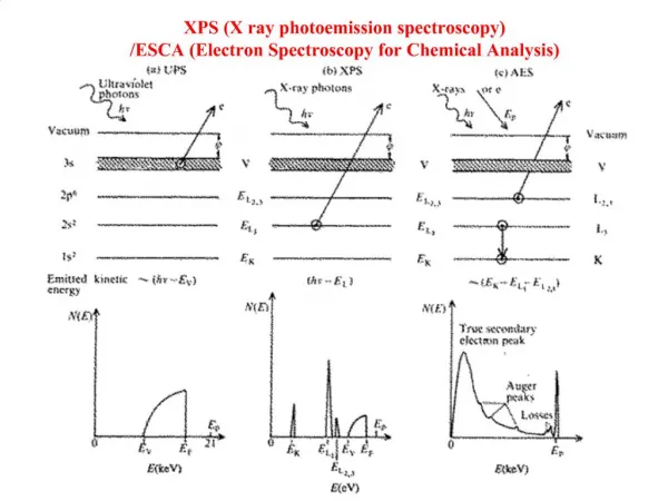
X-Ray Photoelectron Spectroscopy (XPS). Prof. Paul K. Chu. X-ray Photoelectron Spectroscopy. Introduction Qualitative analysis Quantitative analysis Charging compensation Small area analysis and XPS imaging Instrumentation Depth profiling Application examples. Photoelectric Effect.

E N D
X-Ray Photoelectron Spectroscopy (XPS) Prof. Paul K. Chu
X-ray Photoelectron Spectroscopy Introduction Qualitative analysis Quantitative analysis Charging compensation Small area analysis and XPS imaging Instrumentation Depth profiling Application examples
Photoelectric Effect Einstein, Nobel Prize 1921 Photoemission as an analytical tool Kai Siegbahn, Nobel Prize 1981
XPS is a widely used surface analysis technique because of its relative simplicity in use and data interpretation.
KE = hn - BE - FSPECT BE = hn - KE - FSPECT hu: Al Ka(1486.6eV) P 2s P 2p1/2-3/2 Kinetic Energy
For p, d and f peaks, two peaks are observed. The separation between the two peaks are named spin orbital splitting. The values of spin orbital splitting of a core level of an element in different compounds are nearly the same. The peak area ratios of a core level of an element in different compounds are also nearly the same. Au Spin orbital splitting and peak area ratios assist in elemental identification
General methods in assisting peak identification (1)Check peak positions and relative peak intensities of 2 or more peaks (photoemission lines and Auger lines) of an element • Check spin orbital splitting and area ratios for p, d, f peaks A marine sediment sample from Victoria Harbor Si 2p Si 2s The following elements are found: O, C, Cl, Si, F, N, S, Al, Na, Fe, K, Cu, Mn, Ca, Cr, Ni, Sn, Zn, Ti, Pb, V Al 2s Al 2p
Analysis Depth Inelastic mean free path (l) is the mean distance that an electron travels without energy loss For XPS, is in the range of 0.5 to 3.5 nm Only the photoelectrons in the near surface region can escape the sample surface with identifiable energy Measures top 3 or 5-10 nm
Redistribution of electron density B.E. provides information on chemical environment
Factors Affecting Photoelectron Intensities For a homogenous sample, the measured photoelectron intensity is given by Ii,c: Photoelectron intensity for core level c of element i f: X-ray flux in photons per unit area per unit time Ni: Number of atoms of element i per unit volume si,c: Photoelectric cross-section for core level c of element i l: Inelastic mean free path of the photoelectron in the sample matrix q: Angle between the direction of photoelectron electron and the sample normal F: Analyzer solid angle of acceptance T: Analyzer transmission function D: Detector efficiency A: Area of sample from which photoelectrons are detected
Quantitative Analysis Peak Area of element A Sensitivity factor of element A Peak Areas / Sensitivity factors of all other elements Au 4f Peak Area measurement Need background subtraction
Empirical Approach Usually assume SF=1 For example, Teflon (-CF2-)
Examples of Sensitivity Factors N = number of compounds tested
X-ray damage Some samples can be damaged by x-rays For sensitive samples, repeat the measurement to check for x-ray damage.
Charging Compensation Electron loss and compensation
Note: for conducting samples, charging may also occur if there is a high resistance at the back contact.
Charge Compensation Techniques Low Energy Electron Flood Gun
Electron source with magnetic field Low energy electrons and Ar+ A single setting for all types of samples
Instrumentation • Electron energy analyzer • X-ray source • Ar ion gun • Neutralizer • Vacuum system • Electronic controls • Computer system Ultrahigh vacuum < 10-9 Torr (< 10-7 Pa) • Detection of electrons • Avoid surface reactions/ contamination
X-ray monochromator Advantages of using x-ray monochromator • Narrow peak width • Reduced background • No satellite & ghost peaks
Cylindrical Mirror Analyzer CMA: Relatively high signal and good resolution ~ 1 eV
Concentric Hemispherical Analyzer (CHA) Resolution < 0.4 eV
Vacuum Chamber Control Electronics Ion pump Turbopump Sample Introduction Chamber
X-ray induced secondary electron imaging for precise location of the analysis area x-ray secondary electrons + 1 + 2 500 x 500mm
Depth Profiling Sputtered materials Peak Area Sputtering Time
Depth Scale Calibration • Sputtering rate determined from the time required to sputter through a layer of the same material of known thickness • After the sputtering analysis, the crater depth is measured using depth profilometry and a constant sputtering rate is assumed Peak Area Concentration Sputtering Time Depth
Plasma Treated Polystyrene Angle-Resolved XPS Analysis High-resolution C 1s spectra
Plasma Treated Polystyrene • O concentration is higher near the surface (10 degrees take off angle) • C is bonded to oxygen in many forms near the surface (10 degrees take off angle) • Plasma reactions are confined to the surface
Depth Profiling Architectural Glass Coating • Architectural glass coating • ~100nm thick coating Sputtered crater Sample platen 75 X 75mm
Depth profile of Architectural Glass Coating 100 80 O 1s O 1s O 1s 60 Ti 2p Atomic Concentration (%) 40 Nb 3d N 1s Ti 2p Si 2p Si 2p N 1s 20 Al 2p 0 0 200 Surface Sputter Depth (nm)
100 80 Atomic Concentration (%) 60 Ni 2p Cr 2p metal Cr 2p oxide Ni 2p Cr 2p metal Si 2p 40 O 1s 20 0 185 Sputter Depth (nm) 0 Nickel (30.3 nm) Depth profiling of a multilayer structure Chromium (31.7 nm) Chromium Oxide (31.6 nm) Nickel (29.9 nm) Chromium (30.1 nm) Silicon (substrate)
Depth Profiling with Sample Rotation Ions: 4 keV Sample still Cr/Si interface width (80/20%) = 23.5nm Ions: 4 keV With Zalar rotation Cr/Si interface width (80/20%) = 11.5nm Ions: 500 eV With Zalar rotation Cr/Si interface width (80/20%) = 8.5nm
Multi-layered Drug Package Optical photograph of encapsulated drug tablets SPS Photograph Cross-section of Drug Package Al foil Polymer Coating ‘A’ Polymer Coating ‘B’ Adhesion layer at interface ? 100 X 100mm 1072 X 812µm