Download
1 / 21
250 likes | 425 Views
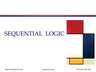
SEQUENTIAL LOGIC. Introduction to Sequential Circuits. Outputs. Inputs. Combina-tional Logic. Storage Elements. Next State. State. A Sequential circuit contains: Storage elements: Latches or Flip-Flops Combinatorial Logic:

E N D
Introduction to Sequential Circuits Outputs Inputs Combina-tional Logic Storage Elements Next State State • A Sequential circuit contains: • Storage elements:Latches or Flip-Flops • Combinatorial Logic: • Implements a multiple-output switching function • Inputs are signals from the outside. • Outputs are signals to the outside. • Other inputs, State or Present State, are signals from storage elements. • The remaining outputs, Next State are inputs to storage elements.
Introduction to Sequential Circuits Outputs Inputs Combina-tional Logic Storage Elements Next State State • Combinatorial Logic • Next state functionNext State = f(Inputs, State) • Output function (Mealy)Outputs = g(Inputs, State) • Output function (Moore)Outputs = h(State) • Output function type depends on specification and affects the design significantly
Types of Sequential Circuits • Depends on the times at which: • storage elements observe their inputs, and • storage elements change their state • Synchronous • Behavior defined from knowledge of its signals at discrete instances of time • Storage elements observe inputs and can change state only in relation to a timing signal (clock pulses from a clock) • Asynchronous • Behavior defined from knowledge of inputs an any instant of time and the order in continuous time in which inputs change • If clock just regarded as another input, all circuits are asynchronous! • Nevertheless, the synchronous abstraction makes complex designs tractable!
Discrete Event Simulation • In order to understand the time behavior of a sequential circuit we use discrete event simulation. • Rules: • Gates modeled by anideal(instantaneous) function and a fixed gate delay • Any change in input values is evaluated to see if it causes a change in output value • Changes in output values are scheduled for the fixed gate delay after the input change • At the time for a scheduled output change, the output value is changed along with any inputs it drives
SR FLIP-FLOP ( SR: set/reset) Q • SR: 01 will always give Q:l SET • SR: 10 will always give Q:0 RESET • SR: 11 will leave Q unchanged: • if Q was SET it remains SET • if Q was RESET it remains RESET • SR : 00 is never used, Q:l but both outputs are equal S (set) Q R (reset)
Clocked S - R Latch • Adding two NANDgates to the basicS - R NAND latchgives the clockedS – R latch: • Has a time sequence behavior similar to the basic S-R latch except that the S and R inputs are only observed when the line C is high. • C means “control” or “clock”. • When CLOCK = 1 the gatesU l andU 2 pass the inverted inputs of S and R to the SRFF . • When CLOCK = 0 the gatesUl and U2 block the inputs, giving a 11 input to the FF. to the SR FF. Note that the inputs are now active HIGH, and the store condition is now 00
Flip-Flop Problem • The change in the flip-flop output is delayed by the pulse width which makes the circuit slower or • S and/or R are permitted to change while C = 1 • Suppose Q = 0 and S goes to 1 and then back to 0 with R remaining at 0 • The master latch sets to 1 • A 1 is transferred to the slave • Suppose Q = 0 and S goes to 1 and back to 0 and R goes to 1 and back to 0 • The master latch sets and then resets • A 0 is transferred to the slave • This behavior is called 1s catching
Flip-Flop Solution • Use edge-triggering instead of master-slave • An edge-triggered flip-flop ignores the pulse while it is at a constant level and triggers only during a transition of the clock signal • Edge-triggered flip-flops can be built directly at the electronic circuit level, or • A master-slave D flip-flop which also exhibits edge-triggered behavior can be used.
Edge-Triggered D Flip-Flop D D S Q Q Q C C C Q R Q Q • The edge-triggered D flip-flop is thesame as the master-slave D flip-flop • It can be formed by: • Replacing the first clocked S-R latch with a clocked D latch or • Adding a D input and inverter to a master-slave S-R flip-flop • The delay of the S-R master-slave flip-flop can be avoided since the 1s-catching behavior is not present with D replacing S and R inputs • The change of the D flip-flop output is associated with the negative edge at the end of the pulse • It is called a negative-edge triggered flip-flop
Positive-Edge Triggered D Flip-Flop • Formed byadding inverterto clock input • Q changes to the value on D applied at the positive clock edge within timing constraints to be specified • Our choice as the standard flip-flop for most sequential circuits
JK FF This is a special flip flop calleda "JK flip flop" whichissimilar to the SR but does not have a forbiddencondition. It is edge-triggered. The 11 inputconditionhasbeendesignedto performa “an output toggle”. Toggle means each clock edge will cause Q to change its logic value
Example 1 x A Q D A Q C B Q D CP Q C y • Input: x(t) • Output:y(t) • State: (A(t), B(t)) • What is the Output Function? • What is the Next State Function?
Example 1 (continued) • Boolean equations for the functions: • A(t+1) = A(t)x(t) + B(t)x(t) • B(t+1) = A(t)x(t) • y(t) = x(t)(B(t) + A(t)) x A Q D A Q C Next State B Q D CP Q' C y Output
Example 1 (continued) 1 0 1 0 0 0 1 0 • Where in time are inputs, outputs and states defined?
Example 1 (continued) State Table Characteristics • State table – a multiple variable table with the following four sections: • Present State – the values of the state variables for each allowed state. • Input – the input combinations allowed. • Next-state – the value of the state at time (t+1) based on the present state and the input. • Output – the value of the output as a function of the present state and (sometimes) the input. • From the viewpoint of a truth table: • the inputs are Input, Present State • and the outputs are Output, Next State
Example 1 (continued) State Table Characteristics Present State Input Next State Output A(t) B(t) x(t) A(t+1) B(t+1) y(t) 0 0 0 0 0 0 0 0 1 0 1 0 0 1 0 0 0 1 0 1 1 1 1 0 1 0 0 0 0 1 1 0 1 1 0 0 1 1 0 0 0 1 1 1 1 1 0 0 • The state table can be filled in using the next state and output equations: A(t+1) = A(t)x(t) + B(t)x(t) B(t+1) =A (t)x(t) y(t) =x (t)(B(t) + A(t))
Example 1 (continued) Alternate State Table Present Next State Output State x(t)=0 x(t)=1 x(t)=0 x(t)=1 A(t) B(t) A(t+1)B(t+1) A(t+1)B(t+1) y(t) y(t) 0 0 0 0 0 1 0 0 0 1 0 0 1 1 1 0 1 0 0 0 1 0 1 0 1 1 0 0 1 0 1 0 • 2-dimensional table that matches well to a K-map. Present state rows and input columns in Gray code order. • A(t+1) = A(t)x(t) + B(t)x(t) • B(t+1) =A (t)x(t) • y(t) =x (t)(B(t) + A(t))
Example 2: Sequential Circuit Analysis A D Z Q Q C R B D Q Q C R C D Q Clock Q C R Reset • Logic Diagram:
Example 2: Flip-Flop Input Equations • Variables • Inputs: None • Outputs: Z • State Variables: A, B, C • Initialization: Reset to (0,0,0) • Equations • A(t+1) = Z = • B(t+1) = • C(t+1) =