Download
1 / 28
280 likes | 440 Views
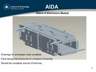
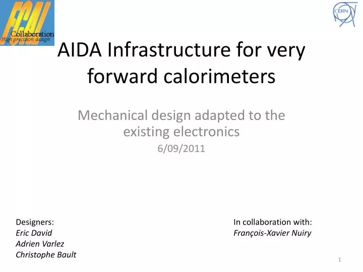
AIDA Infrastructure for very forward calorimeters. Mechanical design adapted to the existing electronics 6/09/2011. Designers: In collaboration with: Eric David François-Xavier Nuiry Adrien Varlez Christophe Bault . AIDA Infrastructure for very forward calorimeters.

E N D
AIDA Infrastructure for very forward calorimeters Mechanical design adapted to the existing electronics 6/09/2011 Designers: In collaboration with: Eric David François-Xavier Nuiry Adrien Varlez Christophe Bault
AIDA Infrastructure for very forward calorimeters Introducing Permaglas frames for higher flexibility 6/09/2011 Slides were re-arranged and slightly modified by K. Elsener Designers: In collaboration with: Eric David François-Xavier Nuiry Adrien Varlez Christophe Bault
Reminder – last FCAL meeting Proposed mechanical infrastructure to allow -> tungsten plates separated by 2 mm or by 1 mm (challenge: ± 50 mm) -> option of 0.5 mm separation is still kept (different design, very preliminary) NB1. sensor position between tungsten plates deemed less critical NB2. structure must accept present LumiCal sensor board and electronics 220mm 78mm 192mm 240mm • Need lateral space • Don’t want to buy larger tungsten plates • Permaglass frames • (sometimes known as Stesalit)
result: new mechanical design 212mm 220mm 78mm 255mm 192mm 240mm 368mm Former design (May 2011, Predeal) 200mm Main structure: New design new dimensions, adapted to the existing electronics
The existing electronics board, in the Permaglas frame [RESARM company] Permaglas frame Glass fibres in epoxy resin PCB Board Comb
The existing electronics board, in the Permaglas frame Proposal – to be discusssed: the PCB should be machined before mounting the Si detector
The tungsten plate, in the Permaglas frame Tungsten Permaglas frame Hinge: Brass Frame: Aluminium Combs: Silvered steel
Tungsten holder: Some details Tungsten Permaglas frame Glued insert
Example: what we can do with C=1mm(present electronics) We work with a step of 4.5mm Electronic board Electronic board Electronic board ~10.5 ~10.5 ~10.5 A=3.5 ~2.5 ~2.5 ~2.5 BEAM Sensor Sensor Sensor C=1 Tungsten plate 125*145 Gap=4.5 Gap=4.5 Gap=4.5 Gap=4.5 Gap=4.5 Gap=4.5 Gap=4.5 Gap=4.5 Gap=4.5 No sensor In this gap No sensor In this gap No sensor In this gap No sensor In this gap No sensor In this gap
Example: detail of arrangement for C=2mm W W 3.5 3.5 C=2 3 2.5 Comb W W With Permaglas frame: 3.7 0.1 3.5 3.5 C=2 3 0.5 2.5
Mechanical infrastructure – general view Horizontal beam Vertical beam (cosmics) The “black box” around this assembly, as specified “light tight”, will be designed soon. This box will also provide means to hold cables and pipes firmly in place (avoid strain on electronics board.
Mechanical frame: Summary • The C=2 solution is designed in full detail • The C=1 solution needs adapted combs, with the same frame (should be designed soon) • The “black box” needs to be designed • We will soon determine the total price of this detector (W + frame) [Approximation] • We will soon meet a subcontractor for all the parts of the mechanical infrastructure
The Future... C=0.5mm • The idea: • We use the same tungsten plates • We could use the same Permaglas frame (in white in this picture) • We glue the Si detector + the read-out on the Permaglas frame • We could realise a sliding kinematic between each tungsten plate, in order to reach the 0.5mm gap between each W plate. • A new mechanical frame is mandatory
The Future... C=0.5mm The most important for us: Realising a flexible link between the sensor and the read out. Something similar to this example (taken from TOTEM): Silicon sensor Connector for the read out Flexible part Rigid part (PCB)
Part 2 - Tungsten plates • Main supplier: Cime Bocuse (Plansee) Tungsten alloys are 4 time cheaper than pure tungsten
Tungsten machining tests: surfacing Is it reproducible? not so sure! An other test is currently done, with a more suitable tool. Diamond + Vitreous matrice instead of Diamond + Bronze matrice
Tungsten machining tests: spot facing Very good result with a standard carbide tool
Tungsten machining tests: Spark machining Very bad results with standard milling tool Very good results with Spark machining
Tungsten procurement News • A new supplier has been identified: ATI Firth Sterling, USA • It proposes tungsten alloys • Other potential suppliers: • STEINEMANN CARBON AG • EWG Wagener www.ewagener.de • www.mgsanders.co.uk Will be tested soon!
Summary (I) – Mechanical Structure • The C=2mm and C=1mm design are nearly ready for us • We will launch a call for tenders for the machining of parts ASAP • The shortest schedule we can propose: • [if subcontractors are available] • We should get the parts for the first mechanical frame with combs for C = 2 mm machined by end of November • We should be able to assemble the frame by mid of January
Summary (II) – tungsten • Machining pure tungsten is too difficult • Machining tungsten alloys is now a priority • In first approximation, a tungsten alloy machined solution is 4 times cheaper than a pure W machined solution • The shortest schedule we can propose: • [if subcontractors are available] • We should get the first machined W alloy plates by end of October (test plates!) • Collaborators will soon be sent a drawing with tungsten plate specifications – you are then encouraged to contact “your” tungsten suppliers to receive offers (details to be discussed)
Additional information about the frame C=2mm We work with an offset of 5.5mm C=1mm We work with an offset of 4.5mm A=3.5 A=3.5 Distance before next tungsten Distance before next tungsten BEAM C=1 C=2 Tungsten plate 125*145 Tungsten plate 125*145 Gap=4.5 Gap=5.5
Additional information about the frame What we can do with C=2mm: We work with an offset of 5.5mm Electronic board Electronic board Electronic board ~10.5 ~10.5 ~10.5 A=3.5 ~2.5 ~2.5 ~2.5 BEAM Sensor Sensor Sensor Tungsten plate 125*145 C=2 C=2 Gap=5.5 Gap=5.5 Gap=5.5 Gap=5.5 Gap=5.5 Gap=5.5 Gap=5.5 No sensor In this gap No sensor In this gap No sensor In this gap No sensor In this gap
Additional information about the frame What we can do with C=2mm: We work with an offset of 5.5mm Electronic board Electronic board Electronic board Electronic board ~10.5 ~10.5 ~10.5 A=3.5 ~2.5 ~2.5 ~2.5 BEAM Sensor Sensor Sensor Tungsten plate 125*145 C=2 Gap=5.5 Gap=5.5 Gap=5.5 Gap=5.5 Gap=5.5 Gap=5.5 Gap=5.5 Gap=5.5 No sensor In this gap No sensor In this gap No sensor In this gap No sensor In this gap
Comments: • Able to work with distance between tungsten plates C=2 mm and 1 mm • This is not viable for the C=0.5 mm version: manufacturing combs is impossible in this case. (Multi-parts structure (internally called ST0362847)) 212mm 220mm 78mm 255mm 192mm 240mm 368mm Former design (May 2011, Predeal) 200mm Main structure: New design new dimensions, adapted to the existing electronics