Download
1 / 36
360 likes | 395 Views
Explore the structure of transistors, digital vs. analog applications, fabrication processes, and practical examples like inverters. Learn about Nobel laureates Shockley, Bardeen, & Brattain. Gain insights into transistor functionality and fabrication techniques worldwide.

E N D
Lecture 4 Transistor as Switch Jan. 13 2003
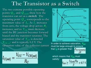
Topics • Transistor structures. • Transistor as a switch
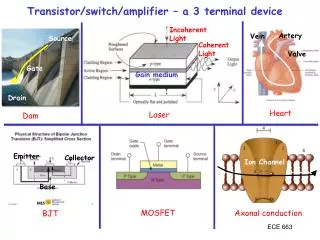
Transistor structure n-type transistor:
The Nobel Prize in Physics 1956 • William Bradford Shockley • Semiconductor Laboratory of Beckman Instruments, Inc. Mountain View, CA, USA • John Bardeen • University of Illinois Urbana, IL, USA • Walter Houser Brattain • Bell Telephone Laboratories Murray Hill, NJ, USA
Transistor • Digital: switch • Analog: many characteristics • Example: inverter • P transistor + N transistor == one inverter
Inverter + out a
VDD tub ties transistors GND Inverter layout + (tubs not shown) out a a out
Example 1 + out b a Write the truth Table of this circuit?
VDD tub ties GND NAND layout + out out b a b a
Example 2 + Write the truth Table of this circuit? b a out
NOR gate + b a out
VDD tub ties GND NOR layout b a b out out a
Difference of digital and analog • Digital: switch • High level • Analog: characteristics of transistor • Low level
Example 3 Transmission gate:
Lecture 5 Transistor Fabrication Process Jan. 15 2003
Topics • Transistor structure (switch) • Basic fabrication steps.
Transistor structure n-type transistor:
Fabrication services • Educational services: • U.S.: MOSIS • EC: EuroPractice • Taiwan: CIC • Japan: VDEC • Fab companies: mainly South Asia
Fabrication processes • IC built on silicon substrate: • some structures diffused into substrate; • other structures built on top of substrate. • Substrate regions are doped with n-type and p-type impurities. (n+ = heavily doped) • Wires made of polycrystalline silicon (poly), multiple layers of aluminum (metal). • Silicon dioxide (SiO2) is insulator.
transistor via Simple cross section SiO2 metal3 metal2 metal1 poly substrate n+ n+ p+ substrate
What is • N and P • Substrate • Poly • Well (tub) • Metal • Via
Photolithography Mask patterns are put on wafer using photo-sensitive material:
Process steps First place tubs to provide properly-doped substrate for n-type, p-type transistors: p-tub p-tub substrate
Process steps, cont’d. Pattern polysilicon before diffusion regions: gate oxide poly poly p-tub p-tub
Process steps, cont’d Add diffusions, performing self-masking: poly poly p-tub n+ n+ p-tub p+ p+
Process steps, cont’d Start adding metal layers: metal 1 metal 1 vias poly poly p-tub n+ n+ p-tub p+ p+
Transistor structure n-type transistor:
Question • How many layers? • Aluminum or copper? • Technology is P-MOS or N-MOS? • What is the purpose of silicon?
Transistor structure (cont’d) n-type transistor:
Questions (cont’d) • Order of Poly !!! • Self-aligned • What is the carrier for N-transistor and P-transistor? • Complete inverter ? • Need metals and vias
0.25 micron transistor (Bell Labs) gate oxide silicide source/drain poly
Review • N transistor • P transistor
Examples • Switch • Fabrication process