Download
1 / 37
370 likes | 406 Views
This resource covers the functional description, activities post-PDR, requirements versus capability, signal flow, board designs, electronics, test results, layouts, analyses, and more in the field of detectors and analog electronics. It details the functional requirements, responsive designs, and board functionalities. The document presents a detailed overview of the detector boards, telescope board, and analog processing board, along with key technical summaries, peer reviews, and future steps. It emphasizes the importance of meeting instrument specifications and capability requirements, with detailed diagrams, interfaces, and detector specifications. The text delves into activities since PDR, summarizing completed tests, simulations, and analysis, ensuring compliance with necessary specifications and verification processes.

E N D
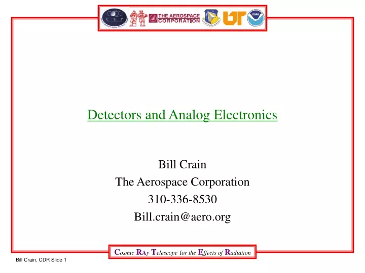
Detectors and Analog Electronics Bill Crain The Aerospace Corporation 310-336-8530 Bill.crain@aero.org
Introduction • Functional Description • Activities since PDR • Requirements vs. Capability • Signal Flow and Interface Block Diagram • Detector and Signal Description • Board Designs • Electronics • Test and simulation results • Layouts • Analyses • Summaries • Peer Review • Next Steps • Conclusion
Functional Requirements • Responsive to Instrument Reqs. Doc. 32-01205 • Functional requirements unchanged since PDR • Measure LET of high LET particles in thin detectors • Measure LET of low LET particles in thick detectors • Provide high energy resolution over range of LETs • Robust to temperature drift and radiation environments • Electronics • Detector Board (detector substrate) • Telescope Board inside Telescope housing • Analog Processing Board (APB) in E-box • No architectural design changes since PDR
Functional Block Diagram Detector Boards Telescope Board Analog Processing Board Thin Preamps Shaping / Scaling Thick Baseline Restorer Bias Networks To Digital Board Thin Discrim. Thick Thermistor Test Pulser Thin Detector Monitor Dosimeter Thick New Since PDR
Activities since PDR • Schematics, layouts, and assembly procedure completed • Breadboard tests performed on preamp and test pulser • Spice simulations performed on shaping amplifier • Tested Micron detectors similar to CRaTER designs • Fabricated and tested engineering model boards • Completed parts derating, thermal stress, and worst-case analyses • Presented electrical design at Goddard peer review
Requirements vs. Capability Summary Electronics design meets requirements derived from Instrument Specification
Bias Network dv/dt & Analog Pulse Silicon Shaping Scaling Preamp Pole-Zero Signals Detector Amp Amp Cancellation Low Lev. Digital Timing Amp Discrim. Signals Test Injection Baseline Restorer Signal Flow Diagram • Single fixed gain linear transfer function • 3 pole pseudo-gaussian response (2 complex, 1 real) • Low level discriminator used for singles counters and coincidence • Baseline restorer corrects for offset drift Analog Board Pulse Processing (1 of 6 strings shown) Telescope Board
Interface Block Diagram • Interface conforms to electrical ICD 32-02052 rev B • Power and bias voltages supplied by digital board • Shaped pulses and discriminator signals supplied by analog board • 78 pin D-sub connector • Added dosimeter HK • Interface Test
Detector Specification (1) • Documented in 32-05001 rev C • No significant changes since PDR • Micron Semiconductor Limited • Lancing, Sussex, UK • Detector Type • Ion-implanted semiconductor doping to form P+ junction on N-type silicon • Good carrier lifetime for thick detectors and excellent depletion layer uniformity • Detector Mount • Attached to small FR4 substrate with low out-gassing adhesive • 3 bond wires per contact • 4 AWG 28 wires (ohmic side, junction contact, guard ring, and ground plane)
Active Dimension (35mm) ~ 1mm Gd/FP P+ Contact Grid Gd/FP P+ implant window 0.1 um Active Volume (depletion region) Thickness 140 um thin; 1,000 um thick E-field N window 0.1 um N contact Detector Specification (2) • Circular detectors having active area of 9.6 cm2 • Two different detector thicknesses: thin and thick • note: state-of-the-art is 20um for thin and 2,000um for thick detectors • Guard ring on P-side to improve surface uniformity
Detector Specification • Detector requirements unchanged since PDR
Detector Issues on Other Programs • Recent problems on STEREO • Failures of flex ribbon cable due to overstress • Leakage current rise in vacuum • CRaTER mitigation • No flex cable. Interconnect wires are light-weight and flexible. • Worst-case analysis demonstrates over 10x margin on leakage current to accommodate drift • Detector screening prior to flight model selection • Keep abreast of latest developments on other programs using Micron detectors • Bi-weekly technical interchange with Micron • Close contact with STEREO science and engineering team at CalTech
Detector Verification • Verification process includes performance tests and environmental tests on all flight detectors • Performance metrics verified by inspection or test per verification plan • Micrometer measurements • Depletion vs. capacitance plots • Leakage current vs. temperature and time plots • Process control data • System test performance • Environmental tests include bond pull, random vibration, thermal cycling, and thermal vacuum (thick only) • All detectors serialized • Stored in dry nitrogen cabinet
RFB CFB Ao Vpk = Qtot/CFB qμnNe(t)E qμpNh(t)E Cdet CFB (Ao) >> Cdet Signal Description • Different signal characteristics for thin and thick detectors are accounted for in design Signal model includes electron and hole drift currents
Introduction • Functional Description • Activities since PDR • Requirements vs. Capability • Signal Flow and Interface Block Diagram • Detector and Signal Description • Board Designs • Electronics • Test and simulation results • Layouts • Analyses • Summaries • Peer Review • Next Steps • Conclusion
Telescope Electronics Design One of six detector strings • Schematic 32-01010 • Detector Bias Network • Detector operates at FD+30V at BOL • Bias network designed to maintain full depletion at worst-case leakage • Preamp • Amptek A250 hybrid • External IF9030 jFET • Connector • Positronic SCBM 24W7 combo-Dsub pigtail • 7 shielded contacts, 18 std Amptek
Telescope Breadboard Test Results (1) • Thin detector preamp • Interfet IF9030 jFET • 15 pF compensation • 0.5 mA bias current • 1 mV / MeV • Thick detector preamp • Interfet IF9030 jFET • 2 pF compensation • 5 mA bias current • 10 mV / MeV
Telescope Breadboard Test Results (2) • Preamp’s full-scale range is 2x below saturation onset test analysis
Telescope Board Layout Bottom Top
Telescope Board Construction • Assembly 32-10101 • Design • Complies with requirements in IPC-2221 and IPC-2222 • 8 layers • Isolated grounds on each preamp • Chassis ground planes on top and bottom • Construction • 0.093 in. finished thickness • Polyimide • Coupons to be sent to MIT and Goddard
Analog Board Electronics (1) To DPB Second-order active filter with signal inversion First-order filter with non-inverting gain From TEL x6 Res + RH1814 RH1814 Unity Gain Buffer x6 RH1814 Res SMB test connector Gain stage X10 Shaping details next slide One-shot ACS14 ACS74 5 us RH1814 Slow integrator RH119 x6 RH1078 Gate Thres Dosimeter Hybrid RH119 <Thres Test Pulser Low Range Current Pulse Detector Leakage Current Amplifier Control Test Pulser High Range To DPB RH1078
Shaping Scaling Pole/Zero Analog Board Electronics (2) • Shaping amplifier • Fast settling • Meets noise requirements • Discriminator • T/N ratio = 10 BOL, 3.2 EOL • Noise occupancy < 0.1% • Baseline Restorer • Gated integrator improves accuracy
Spice Results Actual circuit Monte-carlo Simulation
Analog Board Electronics (3) • Dosimeter • Measures total dose in silicon • 5 mRad increments up to 86 kRad • Utilizes three 5V analog housekeeping channels • Designed by Aerospace internal research project • Approved by LRO QAM as technology demo • Fault-tolerant external interface circuitry • Will not drive CRaTER design, cost, or schedule! Custom charge Integrator ASIC Micron silicon detector
Analog Board Layout Bottom Top
Analog Board Construction • Assembly 32-10101 • Design • Complies with requirements in IPC-2221 and IPC-2222 • 8 layers • Construction • 0.100 in. finished thickness • Polyimide • Coupons to be sent to MIT and Goddard
Introduction • Functional Description • Activities since PDR • Requirements vs. Capability • Signal Flow and Interface Block Diagram • Detector and Signal Description • Board Designs • Electronics • Test and simulation results • Layouts • Analyses • Summaries • Peer Review • Next Steps • Conclusion
Worst-case Analysis • Documented in 32-04011 • Analysis considered temperature and radiation effects • Maximum detector leakage and its effect on bias and noise • Worst-case high LET particle impact on detector and its effect on recovery time and input stage health • Opamp baseline drift and its effects on discriminator accuracy and A/D converter input stability • No performance impact or damage from worst-case predictions
Detector Leakage Effects (1/2) • Designed for worst-case prediction at 35C and 20 krads, per LRO spec 32-01002.0301, and detector proton dose results are in bounds • Detector bias voltage drop constrained to stay above full depletion Ref: J. B. Blake
Detector Leakage Effects (2/2) • Detector thermal noise requirements are met at EOL with a shaping amplifier time constant of 1 usec +/- 20%
High Z Particle Impact Effects • Heavy ions up to Uranium simulated by J. Mazur • Effects on input jFET are non-destructive • Large recovery time constant is incurred on thick detector, but… • Flux is ~10-8 /(m2-sec-sr-MeV/n); on the order of micro-meteorioid strike Ref: Joe Mazur
Op-amp Drift • Used post-irradiated input offset drift specifications from Linear Technologies data sheet • Unacceptable without baseline restorer circuit • Discriminator signal baseline shift 5X threshold • A/D input signal drifts 10X requirement • Baseline restorer solves drift problem • RH1078 has virtually zero input offset drift • Discriminator signal baseline controlled 100X below threshold • A/D input drift limited to less than 0.2% full scale
Parts Stress Analysis • Documented in 32-04010 • Reviewed by Mission Assurance Manager • INST-002 derating requirements satisfied • No thermal stress issues
Radiation Analysis • All op-amps and digital chips are tolerant to over 100 krads as guaranteed by Linear Technologies and Intersil • Datasheet specifications given up to 300 krads • No parts susceptible to latchup • SEU extremely rare • Only digital parts are those used in discriminator one-shot • Intersil parts immune for LET < 100 MeV/cm2/mg • If one did occur, the effect would be one extra count in telemetry. No lockup in analog system.
Peer Review Status • Held at GSFC, May 21, 2006 • Presented detailed schematics of Telescope Board and Analog Processing Board • No action items • Discussion of single-event-transient behavior of opamps and its effect on data
Next Steps • Complete testing of EM electronics • Characterize linearity and noise • Investigate deleterious effects of overload and effects on discriminators • Integrate detectors and run beam test at LBL • Validate signal / noise performance • Include single event transient tests • Deliver EM to MIT • Update layouts for flight • Finalize assembly procedures and electrical test procedures for flight build
Summary • Specifications and ICDs up-to-date • No major revisions since PDR • Breadboard tests show readiness for fabrication • Engineering model board testing going well • Peer review successfully completed