Download
1 / 5
50 likes | 157 Views
Micro-calorimeters Doped - thermistors Astro-E2 6 x 6 pixel array (GSFC/Wisconsin/JAXA) Single pixel work also at Harvard – Smithsonian in collaboration with INAF, Palermo Sub-mm and IR-bolometers (spiderweb) at JPL/Caltech, MPIfR, Bonn and CEA/Saclay (CEA also arrays)

E N D
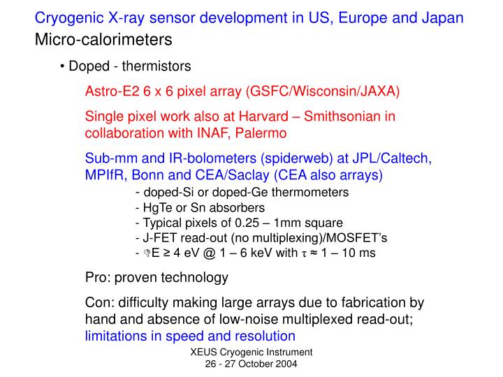
Micro-calorimeters • Doped - thermistors • Astro-E2 6 x 6 pixel array (GSFC/Wisconsin/JAXA) • Single pixel work also at Harvard – Smithsonian in collaboration with INAF, Palermo • Sub-mm and IR-bolometers (spiderweb) at JPL/Caltech, MPIfR, Bonn and CEA/Saclay (CEA also arrays) • - doped-Si or doped-Ge thermometers • - HgTe or Sn absorbers • - Typical pixels of 0.25 – 1mm square • - J-FET read-out (no multiplexing)/MOSFET’s • - E ≥ 4 eV @ 1 – 6 keV with τ ≈ 1 – 10 ms • Pro: proven technology • Con: difficulty making large arrays due to fabrication by hand and absence of low-noise multiplexed read-out; limitations in speed and resolution Cryogenic X-ray sensor development in US, Europe and Japan XEUS Cryogenic Instrument 26 - 27 October 2004
Cryogenic X-ray sensor development in US, Europe and Japan Micro-calorimeters • Phase-transition thermometers (TES) • X-Ray applications Con-X (arrays/TDM/cryogenics) preparations – NIST/GSFC/Wisconsin TES gamma-ray sensors (single pixels) – LLNL XEUS (arrays/FDM) preparations - SRON/MESA/VTT TES single X-ray pixel development – INFN, Genua NEXT/DIOS/XEUS (arrays/FDM) - ISAS/Metropolitan/Waseda • Sub-mm applications Scuba II sub-mm 10.000 pixel array (2005) – NIST/ATC Ground-based sub-mm arrays with TDM – GSFC/NIST Sub-mm bolometer arrays/filters and FDM - UCBerkeley Stanford Optical TES Sub-mm bolometer arrays and read-out - MPIfR, Bonn/JENA Sub-mm TES array/filter development - Cardiff/Cambridge/SRON XEUS Cryogenic Instrument 26 - 27 October 2004
Cryogenic X-ray sensor development in US, Europe and Japan Micro-calorimeters • Phase-transition thermometers (TES) Characteristics • MoCu, TiAu and IrAu TES • Bi absorbers • Typical pixel size 250 x 250 μm2 • Array size up to 8 x 8 • E > 2.8 eV @ 5.9 keV, τ ≈ 0.1 – 1 ms • SQUID amplifiers with TDM or FDM Pro and Con’s Pro: TES is maturing in the 2000 – 2010 timeframe, Large arrays possible from manufacturing and read-out point of view.Potential energy resolution improvement by factor 3: Con: speed limited to about 0.1 ms, pixels larger than 0.5 mm difficult without loss of resolution XEUS Cryogenic Instrument 26 - 27 October 2004
Cryogenic X-ray sensor development in US, Europe and Japan Micro-calorimeters: • Magnetic calorimeters (single pixels so far) Brown Univ/Heidelberg Univ NIST (recently also GSFC started) Characteristics Au:Er thermometers Metallic (Au) absorbers E = 3.4 eV @ 5.9 keV, τ = 60 ms, T = 35 mK, B = 3mT Pro and Cons: Prospect for ≈ 1 eV energy resolution with large absorbers Cons: Sensor speed limited to 0.1 – 1 ms by large heat capacity and e-ph coupling to the bath XEUS Cryogenic Instrument 26 - 27 October 2004
Cryogenic X-ray sensor development in US, Europe and Japan Non-equilibrium sensors: • Superconductive tunnel junctions USA - LLNL (single pixels); Yale (1-D structures) Europe - ESTEC for optical and X-ray applications (single pixels, 1-D/2-D structures, and arrays) PSI, Villigen; TUM, Munich; CNR, Napoli JAPAN - IAST,Tsukuba; Riken, Tokio Characteristics • Ta/AlO/Ta structures most successful • Arrays made up to 18 x 32 • E ≈ 2 eV @ 1 keV and 6 eV @ 6 keV obtained • Typical 25 – 50 micron pixels • Τ ≈ 10 μs Pros: Fast response time and good energy resolution for E < 2 keV Con’s: Difficulty to make large pixels while retaining energy resolution and speed Read-out of large arrays difficult due to magnetic field requirement and lack of adequate multiplexing XEUS Cryogenic Instrument 26 - 27 October 2004