Download
1 / 66
690 likes | 879 Views
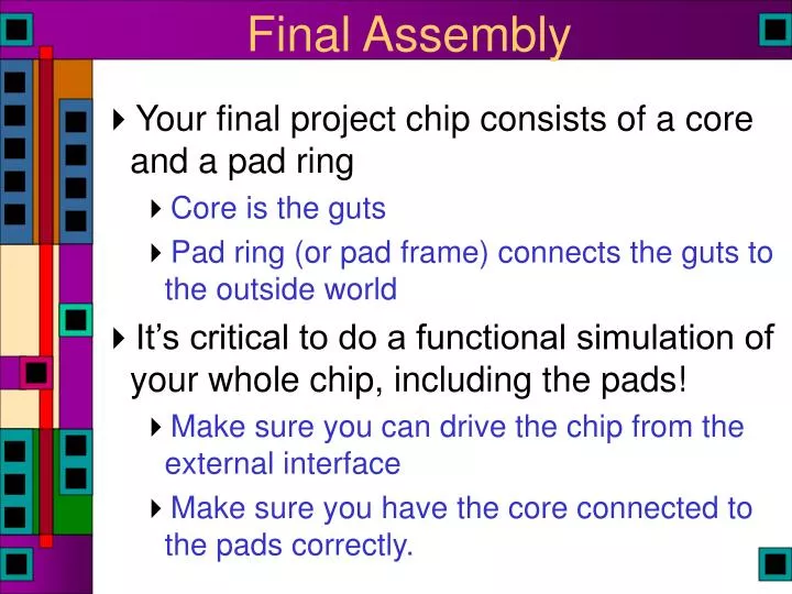
Final Assembly. Your final project chip consists of a core and a pad ring Core is the guts Pad ring (or pad frame) connects the guts to the outside world It’s critical to do a functional simulation of your whole chip, including the pads!

E N D
Final Assembly • Your final project chip consists of a core and a pad ring • Core is the guts • Pad ring (or pad frame) connects the guts to the outside world • It’s critical to do a functional simulation of your whole chip, including the pads! • Make sure you can drive the chip from the external interface • Make sure you have the core connected to the pads correctly.
Chip Core • The Chip Core is everything that is inside the Pad Ring • Try to floorplan your core so that it’s as small a rectangle as possible • At the very least, make sure it fits in the frame you’ve chosen • Make sure to connect vdd and gnd in the core! • This core can be DRC and LVS checked • This core can be simulated for functionality • This core is then routed to the pads
Core Sizes • All things are in terms of Tiny Chip Units (TCUs) • 1 TCU = 1.5x1.5mm outside dimension • 1 TCU = 900x900 usable core area • 2 TCU = 900x2300 usable core area • 4 TCU = 2300x2300 usable core area • More on this later!
Connecting Core to Pads • Once your core is complete, you need to connect it to the pad frame • Then you re-do the functional simulation, but through the pads this time • You should be able to re-use your testfixture • Also a final DRC and LVS which includes the pads • Use ccar for connecting the core to the pads! • Chapter 11 in the CAD manual
Core • The guts of your chip
Pad Ring • The connection to the outside world
Tutorial Example • A tiny state machine in a 1-tiny-chip frame
Pad Cells • Started with a set of pads from MOSIS • Originally from Tanner Tools pads • Problem: the pads don’t DRC, LVS, or simulate! • Cameron Charles re-did the cells in 2002 (as a grad student) to fix these issues • Result is UofU_Pads • /uusoc/facility/cad_common/local/Cadence/lib/UofU_Pads • Use library manager to add this library • Name it UofU_Pads • They now DRC, LVS, and simulate!
Bonding Pad Design Bonding Pad GND 100 mm Out VDD Out In GND
UofU_Pads 255u
UofU_Pads • pad_bidirhe • Bidirectional pad with high enable • pad_in • Digital input pad • pad_out • Digital output pad • pad_vdd, pad_gnd • Power supply pads • pad_io, pad_io_nores • Analog pads (with and without series resistor) • pad_nc, pad_space • Non-connecting pad and spacer
Pad Interfaces pad_bidirhe pad_bidirhe (EN) (DataOut) (DataIn, DataInB) (pad) • DataOut drives a 78(p) x 45(n) inverter (30x) • Which then drives a 200(p) x 200(n) output driver (133x) • DataIn and DataInB come from 96(p) x 54(n) inverters (36x) • EN drives a 16(p) x 9(n) inverter (6x) • All signal pads are built from this one • All signals on are M2
pad_bidirhe • Moderately complex pullup/pulldown structure
pad_bidirhe • M2 connections for EN, DataOut, DataIn, DataInB
pad_bidirhe • Look at just the metal layers… • EN, DataOut, DataInB, DataIn is the order • Middle connection is direct connection to the pad (don’t use it!) • You put metal2 shape pins over the connection points (for icc)
UofU Pads pad_out pad_out (pad) (DataOut) pad_in pad_in (DataIn, DataInB) (pad)
pad_out • Like pad_bidirhe but with EN already tied high for you • All you need to connect is DataOut
pad_out • You connect your signal to the DataOut connection into 78(p) x 45(n) inv (30x)
pad_out • You connect your signal to the DataOut connection into 78(p) x 45(n) inv (30x)
pad_in • Like pad_bidirhe but with EN tied low already for you • Connect to the DataInB and DataIn port
pad_in • DataIn and DataInB provide input signals • Driven from 94(p) x 54(n) inverters (36x)
Power Supply Pads pad_vdd pad_vdd pad_gnd pad_gnd
pad_vdd • Vdd is on a big fat metal1 line • 28.8u wide
pad_gnd • GND is also on a big fat metal1 line • Also 28.8u
Timetable • Final Chip Assembly • Due Friday December 19th • Take the pad cells and make a pad ring • Connect your working core to the pad ring • Remember that Tiny Chip Units are 1.5mm X 1.5mm and are not divisible • A 3.1mm X 2.8mm chip would cost 6 TCUs! • Preference will go to the well-simulated chips • Secondary preference will be for the smaller well-simulated chips
Available Frames • Frame1_38 • Frame2h_70 • Frame2v_70 • Frame4_78 • 1,2,4 indicate how many Tiny Chip Units • h and v indicate horizontal and vertical for the rectangular core frames • _# indicates how many signal pins are available • Vdd and gnd are in the right spots – DON’T MOVE THEM!
Frame1_38 40 pins total(38 signal pins) 10 on each side 990 x 990 core Save room for Routing to pads! 900 x 900 Usable core
Frame1_38 40 pins total(38 signal pins) 10 on each side 990 x 990 core Save room for Routing to pads! 900 x 900 Usable core
Frame1_38 40 pins total(38 signal pins) 10 on each side 990 x 990 core Save room for Routing to pads! 900 x 900 Usable core
Frame2h_68 72 pins total, 70 signal pins 990 x 2430 core (900 x 2300 usable)
Frame2h_68 72 pins total, 68 signal pins 990 x 2430 core (900 x 2300 usable)
Frame4_78 84 total pins (78 signal pins) 2490 x 2490 (2300 x 2300 usable)
Frame4_78 84 total pins (78 signal pins) 2490 x 2490 (2300 x 2300 usable)
How to Use the Rings • Copy the pad ring of your choice • /uusoc/facility/cad_common/local/Cadence/lib/UofU_Pads • From UofU_Pads • To your project directory • Leave the pad_vdd and pad_gnd where they are! • Select other pads, use properties to change to the pad type you want • DON’T move them! • Use pad_bidirhe, pad_out, and pad_in