Download
1 / 26
1.52k likes | 4.24k Views
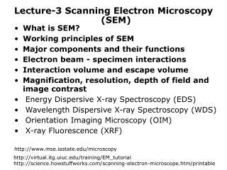
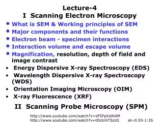
Scanning Electron Microscopy. What is an SEM?. What is an SEM?. A Scanning Electron Microscope is an instrument that investigates the surfaces of solid samples by using a beam of electrons in a vacuum. What is an SEM?.

E N D
What is an SEM? • A Scanning Electron Microscope is an instrument that investigates the surfaces of solid samples by using a beam of electrons in a vacuum.
What is an SEM? • A Scanning Electron Microscope is an instrument that investigates the surfaces of solid samples by using a beam of electrons in a vacuum. • The image is generated by the secondary emissions from the sample.
Advantages of using an SEM instead of a light microscope • Imaging • high resolution (because of short wavelength) - >1.4nm
Advantages of using an SEM instead of a light microscope • Imaging • high resolution (because of short wavelength) - >1.4nm • Secondary electron imaging for topology
Advantages of using an SEM instead of a light microscope • Imaging • high resolution (because of short wavelength) - >1.4nm • Secondary electron imaging for topology • Backscatter electron imaging for chemistry
Advantages of using an SEM instead of a light microscope • Imaging • high resolution (because of short wavelength) - >1.4nm • Secondary electron imaging for topology • Backscatter electron imaging for chemistry • High depth of field
Advantages of using an SEM instead of a light microscope • Imaging • high resolution (because of short wavelength) - >1.4nm • Secondary electron imaging for topology • Backscatter electron imaging for chemistry • High depth of field • Elemental Analysis – EDXS (Energy-dispersive X-ray analysis)
Advantages of using an SEM instead of a light microscope • Imaging • high resolution (because of short wavelength) - >1.4nm • Secondary electron imaging for topology • Backscatter electron imaging for chemistry • High depth of field • Elemental Analysis – EDXS (Energy-dispersive X-ray analysis) • Structural Analysis – EBSD (Electron Back-scatter Diffraction analysis)
Advantages of using an SEM instead of a light microscope • Imaging • high resolution (because of short wavelength) - >1.4nm • Secondary electron imaging for topology • Backscatter electron imaging for chemistry • High depth of field • Elemental Analysis – EDXS (Energy-dispersive X-ray analysis) • Structural Analysis – EBSD (Electron Back-scatter Diffraction analysis) • Ease of sample preparation since most SEMs only require the sample to be conductive.
Sample Constraints • Must fit in chamber (!)
Sample Constraints • Must fit in chamber • Must be compatible with vacuum (even for ESEM samples)
Sample Constraints • Must fit in chamber • Must be compatible with vacuum (even for ESEM samples) • Must have conductive surface (not necessary for ESEM samples)
Secondary Electron Images Give information about sample's topography
BSE Images Give information about sample's chemistry
EDS Spectra Give information about sample's composition
X-Ray Maps Give information about elemental distribution in the sample SE Cu Pb Sn
Electron beam strikes a crystalline material tilted at 70° Backscatter patterns composed of intersecting bands Indexable patterns
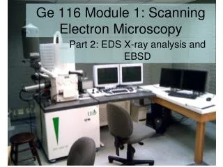
Center for Materials Science and Engineering Electron Microscopy SEF Location: 13-1012 Normal Working Hours:8:30 am – 4:45 pm on M-F 24 hr accessible for evening/weekend users (not for undergraduates) Staff: Dr. Anthony (Tony) Garratt-Reed (TEM, SEM, STEM) Dr. Yong Zhang (TEM, SEM, STEM) Mr. Patrick Boisvert (SEM, Microtome)