Download
1 / 22
230 likes | 417 Views
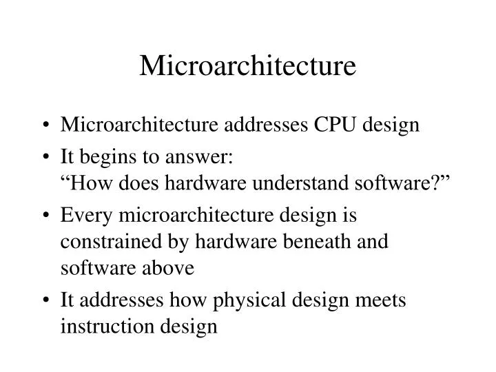
Microarchitecture. Microarchitecture addresses CPU design It begins to answer: “How does hardware understand software?” Every microarchitecture design is constrained by hardware beneath and software above It addresses how physical design meets instruction design. Physical Design of CPU.

E N D
Microarchitecture • Microarchitecture addresses CPU design • It begins to answer:“How does hardware understand software?” • Every microarchitecture design is constrained by hardware beneath and software above • It addresses how physical design meets instruction design
Physical Design of CPU • How do all the pieces communicate? • Buses: outside CPU and inside CPU • How does each piece know what to do? • Control signals • What are all the pieces? • Know your registers • Others: ALU, memory, I/O devices • The master piece: control unit
Registers • User versus system registers • Some essential registers (actual names vary) • MAR = Memory Address Register • MBR = Memory Buffer Register • PC = Program Counter • IR = Instruction Register • Status or Flags Register (e.g. overflow bit) • General purpose registers
Key Data Flows: Fetching • PC has next instruction's address in memory • Control store tells everyone to fetch • Contents of PC sent to memory as address • Memory told to perform read op • Result of read returns to CPU • CPU eventually expects instruction in IR • Some CPUs restrict MAR, MBR as only way to “talk” to memory
Key Data Flows: ALU Operation • Registers in/out connected to bus • ALU in/out connected to bus • Consider steps for “C=A + B” • Load register A onto bus • Load bus into left side of ALU • Load register B onto bus • Load bus into right side of ALU • Tell ALU to do add op (remember talking about this?) • Load ALU result onto bus • Load bus into register C
Steps for MAR=MBR+AC • Load AC onto bus • Load Y from bus • Load MBR onto bus • Load ALU from bus • Tell ALU to do add op • Load Z onto bus • Load MAR from bus
Steps for CPP = LV + TOS • Load LV onto input bus (B bus) • Pass LV through ALU as is (ALU op: B) • Store output bus (C bus) into H • Load TOS onto B bus • ALU adds H and B bus (ALU op: A + B) • Store C bus into CPP
Steps for CPP = LV + TOS • Load LV onto left input bus (A bus) • Load TOS onto right input bus (B bus) • ALU adds A bus and B bus • Store C bus into CPP
Space and Time • There's a sub-plot to this discussion • Often we can gain speed/time, but at a cost • Cost is added circuitry • Takes up more space • Generates more heat • More parts adds to price of building • More complexity may lead to more problems
Of Clocks and Timing • Clock pulse frequency isn’t whole story • Each pulse sub-divided into sub-cycles • Not necessarily pipelined • Possible sub-cycles • Set up control signals (at control store) • Load up bus(es) with ALU inputs from register(s) • Run ALU • Propagate ALU output to bus and to register(s) • Establish values for registers (at rising edge of pulse)
Some Questions • Why does the ALU and shifter have a time delay? How much time delay is it? • What is the ALU doing while the control signals are being set up? • What about the gap after C bus propagation? Is it good or bad? How can we get rid of it?
Many Levels of Translation • Compiler translates high-level instructions (e.g. Java or C) into machine instructions • CPU fetches and decodes one machine instruction • Actual execution typically involves a sequence of microinstructions (some have 100s!) • Control store decodes one microinstruction into a bunch of control signals