Download
1 / 36
380 likes | 503 Views
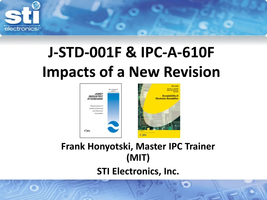
J-STD-001F & IPC-A-610F Impacts of a New Revision. Frank Honyotski, Master IPC Trainer (MIT) STI Electronics, Inc. J-STD-001F What’s New Additions IPC-A-610F What’s New Additions Training. Agenda. What’s New? Format Removed Space Shuttle symbol Layout

E N D
J-STD-001F & IPC-A-610FImpacts of a New Revision Frank Honyotski, Master IPC Trainer (MIT) STI Electronics, Inc.
J-STD-001F What’s New Additions IPC-A-610F What’s New Additions Training Agenda
What’s New? Format Removed Space Shuttle symbol Layout Some requirements relocated for readability Revised Requirements Where data supported a change New Requirements To support industry advance A New Revision of J-STD-001
1.8.3 FOD (Foreign Object Debris) A generic term for a substance, debris, particulate matter or article alien to the assembly or system. J-STD-001 Terms & Definitions FOD
J-STD-001 Requirements Flowdown • 1.9 Requirements Flowdown… • When an assembly, e.g., daughterboard, is procured, that assembly should meet the requirements of this standard. The connections from the procured assembly to the manufactured assembly shall [D1D2D3] meet the requirements of this standard. • If the assembly is manufactured by the same manufacturer, the solder requirements are as stated in the contract for the entire assembly. • The design and workmanship of COTS items should be evaluated and modified as required to ensure the end-item meets contract performance requirements. • Modifications shall [D1D2D3] meet the applicable requirements of this standard.
The balance of an SAC305 lead-free bath shall [N1D2D3] be the items listed in Table 3-1. Use of other lead-free solder alloy contamination limits shall [N1D2D3] be on agreement between Manufacturer and User. Table 3-1 Maximum Limits of Solder Bath Contaminant
3.8.1 Component and Seal Damage • Loss of silver-palladium metallization shall [D1D2D3]: • Not expose ceramic on the terminal end face. • Be no greater than 25% of width or thickness on any termination side (not the end face). • Be no more than 50% on top of a 5 or 3 sided termination component.
4.5.1 Gold Removal • Except as noted above, gold shall [N1PD2D3] be removed: • a. From at least 95% of the surfaces to be soldered of the through-hole component leads with >2.54 μm [100 μin] gold thickness and all through-hole leads that will be hand soldered regardless of gold thickness. • b. From 95% of all surfaces to be soldered of surface mount components regardless of gold thickness. • c. From the surfaces to be soldered of solder terminals plated with >2.54 μm [100 μin] of gold thickness and from all solder cup terminals, regardless of gold thickness.
Table 4-1 added to include solder anomalies not just defects. Table 4-1 Solder Anomalies Solder Connection Anomalies Note 1: Solder in the bend radius is not cause for rejection provided the lead is properly formed and the topside bend radius is discernible.
Jumper Wires • 5.6 Jumper Wires Jumper wires shall [N1D2D3] be permitted only by drawing(s)/engineering documentation or other contractual action. When the criteria for jumper wires is not specified by engineering documentation, the requirements of 5.6.1 through 5.6.6.4 shall [N1D2D3] apply. See IPC-7711/7721 and IPC-A-610 for additional information. • Jumper wire information now matches 610.
Through-Hole Mounting and Terminations • Table 6-2 Components with spacers added to through-hole. Table 6-2 Components with Spacers
Hold Down of Surface Mount Leads/Components • 7.4 Hold Down of Surface Mount Leads/Components • Surface mounted device leads or components shall not [N1N2D3] be pressed down against the PCB land or other mating surface during the soldering operation or during solder solidification. • NOTE: Mechanically constrained devices such as connector securing tabs or holding a part over a pad from the sides during soldering is not the same as pressing the component down to the land.
Butt/I Connection-Solder Charged Termination (NEW) • 7.5.10.2 Butt/I Connections – Solder Charged Terminations • These criteria are for components designed with a hole or holes in the lead, a bump on the bottom to assure a good (G) fillet thickness across most of the bottom, and an attached solder slug to control the amount of solder. Connections formed to solder-charged leads positioned perpendicular to a circuit land in a butt/I configuration shall [D1D2D3] meet the dimensional and solder fillet requirements of Table 7-11; see Figure 7-11.
P-Style Terminations(NEW) • 7.5.18 P-Style Terminations • Connections formed to components having the P-Style termination (Figure 7-19) shall [D1D2D3] meet the dimensional and solder fillet requirements of Table 7-21. This termination style is typically found on edge mounted connectors that will be soldered on both sides of the board.
P-Style Terminations(NEW) Table 7-21 Dimensional Criteria – P-Style Terminations
10 Coating, Encapsulation and Staking(Adhesive) • Entire section reworded and new criteria added.
Witness (Torque/ Anti-Tampering) Stripe (NEW) • 11 Witness (Torque /Anti-Tampering) Stripe • If torque (witness/anti-tampering) stripe is required, the following criteria shall [N1N2D3] be used: • a. Be continuous between the fastener and the substrate. • b. Be undisturbed. • c. Extend from the top of the fastener onto the adjacent substrate (at minimum). • d. Be aligned with the center line of the fastener.
Appendix C(NEW) • J-STD-001 Guidance on Objective Evidence of Material Compatibility • Overview • Most electronics assembly operations are a series of mechanical, thermal, and chemical processes, each having a potentially adverse effect on the long term functionality and reliability of the assembled product. • The average electronic assembly will have been subjected to at least 20 different chemical processes, many employing especially aggressive chemicals. • To accurately determine that mixtures of these various chemicals do not produce adverse effects, the Manufacturer needs to have examined chemical interactions within their chosen material sets. J-STD-001 has always required that “objective evidence” of “chemical compatibility” be on hand for review. • This appendix was generated by a focus group of the J-STD-001 committee to generate guidance on this issue.
Personnel Proficiency(NEW) • 1.3 Personnel Proficiency • All instructors, operators, and inspection personnel shall be proficient in the tasks to be performed. • Objective evidence of that proficiency shall be maintained and available for review. • Objective evidence should include records of training to the applicable job functions being performed, work experience, testing to the requirements of this standard, and/or results of periodic reviews of proficiency. • Supervised on-the-job training is acceptable until proficiency is demonstrated.
Supported Holes- Solder • Added criteria for Class 2 vertical fill for components with 14 or more leads and Less than 14 leads.
Chip Components – Billboarding • Changed the Class 3 Acceptable criteria. • For components size 1206 or smaller: • Component has 3 or more termination faces (metallization).
8.3.5 Flat Gull Wing Leads • Maximum Toe Overhang for Class 2,3 • Not permitted when (L) is less than 3 (W)
Butt/I Connections- Solder Charged Terminations(NEW) • Same as J-STD-001F
P-Style Connections(NEW) • Same as J-STD-001F
9.2 Chip Resistor Element • Acceptable – Class 1, 2, 3 • No damage to the resistive element or glass coating. • No exposure of the resistive element. • Reference to 1206 size component removed.
9.13 Threaded Items and Hardware (NEW) • Defect - Class 1,2,3 • Evidence of damage resulting from over-tightening of the threaded item.
10.2.4 Laminate Conditions - Haloing • Criteria separated from edge delamination. • Edge delamination combined with Nicks and crazing.
10.4 Flexible and Rigid-Flex Printed Circuitry • Criteria changed to more closely align with IPC-A600.
10.5.5.2 Marking – Labels – Readability • Removed the laser and wand type scanner and replaced with code can be read with 3 or fewer attempts.
10.8.4 Electrical Insulation Coating (NEW) • This material is used to provide insulation to an exposed conductor when conformal coating is insufficient to provide enough protection and encapsulation is too much. • All of the considerations used for conformal coating are applicable for insulation coating, except the surface where insulation coating is applied is generally not smooth enough for a uniform coating surface. • Thin coating is not a target attribute. See 10.5.2.2
10.8.4 Electrical Insulation Coating (NEW) • The material used is frequently a conformal coat like material with a thickener added. • Example: • Bolted solder lugs where the edge surface is not fully protected by conformal coating • Component cases that are electively active • Wire termination, particularly moveable wires
J-STD-001F Certification CourseIPC-A-610F Certification Course • J-STD-001 Certified IPC Trainer (CIT) and Certified IPC Application Specialist (CIS) Training Courses • Currently under development • CIT Beta class to be held December 8-12, 2014 • IPC-A-610 CIT and CIS Training Courses • Currently under development • CIT Beta class to be held February 2-6, 2015