Download
1 / 39
390 likes | 515 Views
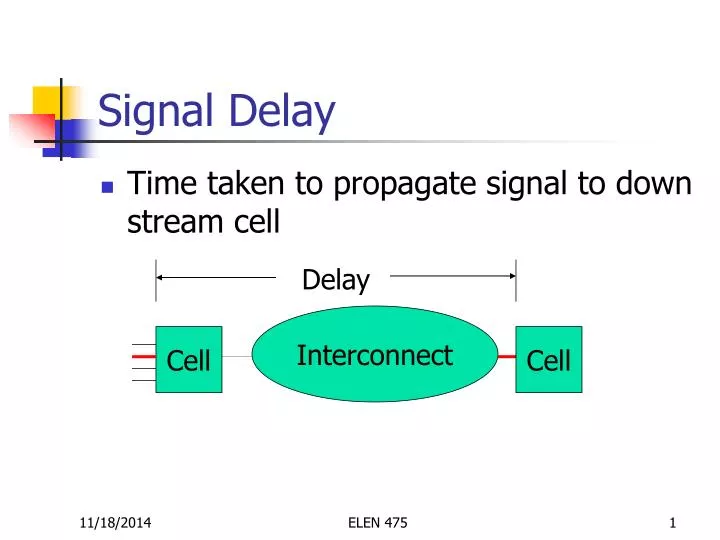
Signal Delay. Time taken to propagate signal to down stream cell. Delay. Interconnect. Cell. Cell. Terminology. Rise time t r : time for a waveform to rise from 10% to 90% Vdd Fall time t f : time for a waveform to fall from 90% to 10% Vdd

E N D
Signal Delay • Time taken to propagate signal to down stream cell Delay Interconnect Cell Cell ELEN 475
Terminology • Rise time tr: time for a waveform to rise from 10% to 90% Vdd • Fall time tf: time for a waveform to fall from 90% to 10% Vdd • Delay tdf, tdr: time difference between input and output transition (50%) • Be aware of negative delay! ELEN 475
Example 90% tdf tdr 50% 10% tf tr Vout(t) Vin(t) ELEN 475
Fall Time Analysis • Assumption: Vgs goes from 0 to Vdd in no time • Time tf1: In saturation region, Vout drops from 0.9Vdd to (Vdd–Vtn) • Time tf2: In linear region, Vout drops from (Vdd – Vtn) to 0.1Vdd Ic Vout CL n-device ELEN 475
Saturation Region • Discharging current is constant ELEN 475
Fall time tf1 ELEN 475
Linear Region • Discharging current no longer constant ELEN 475
Fall Time tf2 • Let n=Vtn/Vdd, ELEN 475
Total Fall Time • Sum of tf1 and tf2 ELEN 475
Total Rise Time • Similarly, let p=|Vtp|/Vdd ELEN 475
Delay • Delay at 50% Vdd can be approximated • Rising delay tdr=tr/2 • Falling delay tdf=ft/2 • For inverters/buffers, tdr can be made to equal tdf, but for other types of devices it is hard, especially with side input. ELEN 475
Other Complications • Input rises slowly • Both p-MOS and n-MOS may be on • When n-MOS is in saturation region, p-MOS might be in linear region • Side input coming at the same time, with skew and different slope • Gate input capacitance Cg=Cgd+Cgs+Cgd is not a constant ELEN 475
Standard Cell Design • Standard Cell Design uses a cell library provided by the foundry • A cell library contains a few hundreds cells • However, in modern design the cells will be resized to optimize delay and power ELEN 475
Empirical Methods for StdCell • Linear delay d=d0+fCL • For each fixed input slope, run SPICE simulation on different Cl and find a best linear approximation delay CL ELEN 475
Non-Linear: K-factor • Consider input transition time tr/f • Transition time is signal rising/falling time from 10% to 90% or 20% to 80% • K-factor equation • Delay td=k(tr/f, Ctotal) • Output transition time t’r/f=k’(tr/f, Ctotal) rising time ELEN 475
K-Factor … • Synopsis K-factor form: • Piece-wise-quadratic • For each piece, a*tr+b*Ctotal+c*tr*Ctotal+d • Obtained from SPICE simulation • Ignore interconnect resistance shielding • Widely used ELEN 475
Interconnect Delay • Simple RC delay, where R is total resistance of wire and driver and C is total capacitance of wire and sink RC delay 1200*52 100 Rd =1k 100 1 1 50 ELEN 475
Elmore Delay 100 100 100 1000 3 4 1 1 50 60 Elmore Delay td=i RiCi where Ci is the downstream capacitance At output 1: 1000*112 At output 2: 1000*112+100*111 At output 3: 1000*112+100*111+100*50 At output 4: 1000*112+100*111+100*60 ELEN 475
Application of Elmore Delay • Good • Closed form expression, easy to compute • Accuracy is better the ramps • Useful for routing and placement • Bad • Inaccurate • For less than 0.25 um technology • Unbalanced RC trees • Driver ignored • Not useful for timing verification ELEN 475
Gate/Cell Delay • Rising: 2 p-MOS in serial • Falling: 1 n-MOS or 2 n-MOS in parallel Vdd x out y ELEN 475
Driver Resistance • Assume all p-MOS are same size • For 2 p-MOS in serial, neff= n/2 • Assume all n-MOS are same size, • For 2 n-MOS in parallel, neff= 2n • Therefore the rising time is twice the rising of one p-MOS, and the falling delay is half the falling delay of one n-MOS ELEN 475
Side Input • Delay from x to out is different for different values on y • Characterize for all input combinations Vdd x out y ELEN 475
Simultaneous Switching • Too many cases to consider • Big impact on delay Vdd x out y ELEN 475
Transistor Sizing • Re-sized cells are common to minimize delay and/or power ELEN 475
Buffer Insertion and Sizing • One of the most effective way to reduce delay • Consider the simplest version • Slack is the RAT (required arrival time) minus delay Without buffer Delay to s1 is 40, slack is 30-40=-10 Delay to s2 is 50, slack is 60-50=10 Slack at source = min{-10,10}= -10 RAT=60 sink s2 source s0 With buffer Delay to s1 is 20, slack is 30-20=10 Delay to s2 is 30, slack is 60-30=30 Slack at source = min{10,30}= 10 RAT=30 sink s1 ELEN 475
Buffers and Inverters • A buffer consists of two inverter • An inverter is also called “inverting buffer” • Different buffer sizes possible • Different wire width possible ELEN 475
Problem Description • Given: A routing tree, possible buffer positions, sink required arrival times (RAT), wire resistance and capacitance, buffer resistance and capacitance s2 sinks s1 s0 s3 s4 source possible buffer positions ELEN 475
Problem Description • Find: Where to insert buffers so that the slack at the source Q(s0) is satisfied s2 s1 s0 s3 s4 ELEN 475
Linear Delay for Buffer u v u C(b) Cv Driver resistance Input capacitance Intrinsic buffer delay ELEN 475
Elmore Delay for Wire Rw Cw wire capacitance Cw wire resistance Rw v u Cv ELEN 475
How to do it? • At each of the n buffer positions, we can either insert a buffer, or not insert a buffer • So there are 2npossible candidate solutions • Compute the slack for each candidate and pick the best one • Too time consuming even for n>30 ELEN 475
s2 (Q,C) (100,10) (200,20) (300,15) v s1 Van Ginneken’s Algorithm • Each candidate solution of a branch is represented by a (Q, C) pair, where Q is slack, C is capacitance • For two candidates Ai and Aj of the same branch, if Q(Ai)<Q(Aj), and C(Ai)>C(Aj), then Ai is redundant • For example, if there are 3 ways to insert buffers for the net below v, with slacks and capacitance shown • Which candidate(s) is redundant? ELEN 475
Key Ideas • We only need to remember the non-redundant candidates since other candidates will give worse slack • Build the list of non-redundant candidates from sinks towards the source • Bottom-up, aka dynamic programming ELEN 475
Initialization • For each sink si, set one candidate with • Q=required arrival time RAT(si) • C=capacitance of si ELEN 475
Add Wire wire R=10, C=10 s0 (50050300, 30+10) (40050200, 20+10) (30050150, 15+10) (150, 40) (150, 30) (150, 25) (500, 30) (400, 20) (300, 15) ELEN 475
(500, 30) (400, 20) (300, 15) without buffer Add Buffer Buffer R(b)=10, C(b)=10 s0 (500, 30) (400, 20) (300, 15) (200, 10) (200, 10) (150, 10) (500300,10) (400200,10) (300150,10) with buffer ELEN 475
Merge (500, 20) (300, 10) s0 Q=min{Qi,Qj} C=Ci+Cj (500, 30) (400, 20) (300, 15) (250, 10) (500, 20)&(500, 30) = (500, 50) &(400, 20) = (400, 40) &(300, 15) = (300, 35) &(250, 10) = (250, 30) (300, 10)&(500, 30) = (300, 40) &(400, 20) = (300, 30) &(300, 15) = (300, 25) &(250, 10) = (250, 20) ELEN 475
Running Time Analysis • Total number of candidates is n+m • Initialization: At most m new candidates • Add wire: No new candidates • Add buffer: One new candidate for each buffer position, at most n new candidates • Merge: No new candidate • Running time of Van Ginneken’s algorithm is O(n2) ELEN 475
Buffer Sizing • Apply the same algorithm, except with a number of buffers to choose at each buffer insertion position • Cascaded buffers to drive a large load ELEN 475