Download
1 / 51
510 likes | 638 Views
Advance Processor Chapter 3. Prepared by: Prof. Ajaykumar T. Shah. Cache Memory. Program loaded into main memory DRAM which is slower devices. It reduces speed of execution. To speed up the process, high speed memory such as SRAM must be used. Problem: Cost and size.

E N D
Advance ProcessorChapter 3 Prepared by: Prof. Ajaykumar T. Shah Blog: aforajayshahnirma.wordpress.com
Cache Memory • Program loaded into main memory DRAM which is slower devices. • It reduces speed of execution. • To speed up the process, high speed memory such as SRAM must be used. • Problem: Cost and size. • Sol: Small section of SRAM is added along with main memory. It is called as cache memory. • Part of code and data is accessed from cache memory. • This is accomplished by loading active Part of code and data to cache memory Blog: aforajayshahnirma.wordpress.com
What is CISC? • CISC is an acronym for Complex Instruction Set Computer and are chips that are easy to program and which make efficient use of memory. Since the earliest machines were programmed in assembly language and memory was slow and expensive, the CISC philosophy made sense. • Most common microprocessor designs such as the Intel 80x86 and Motorola 68K series followed the CISC philosophy. • But recent changes in software and hardware technology have forced a re-examination of CISC and many modern CISC processors are hybrids, implementing many RISC principles. • CISC was developed to make compiler development simpler. It shifts most of the burden of generating machine instructions to the processor. For example, instead of having to make a compiler write long machine instructions to calculate a square-root, a CISC processor would have a built-in ability to do this. Blog: aforajayshahnirma.wordpress.com
CISC Attributes The design constraints that led to the development of CISC (small amounts of slow memory and fact that most early machines were programmed in assembly language) give CISC instructions sets some common characteristics: • A 2-operand format, where instructions have a source and a destination. Register to register, register to memory, and memory to register commands. Multiple addressing modes for memory, including specialized modes for indexing through arrays • Variable length instructions where the length often varies according to the addressing mode • Instructions which require multiple clock cycles to execute. E.g. Pentium is considered a modern CISC processor Blog: aforajayshahnirma.wordpress.com
Most CISC hardware architectures have several characteristics in common: • Complex instruction-decoding logic, driven by the need for a single instruction to support multiple addressing modes. • A small number of general purpose registers. This is the direct result of having instructions which can operate directly on memory and the limited amount of chip space not dedicated to instruction decoding, execution, and microcode storage. • Several special purpose registers. Many designs set aside special registers for the stack pointer, interrupt handling, and so on. This can simplify the hardware design somewhat, at the expense of making the instruction set more complex. Blog: aforajayshahnirma.wordpress.com
What is RISC? • RISC?RISC, or Reduced Instruction Set Computer. is a type of microprocessor architecture that utilizes a small, highly-optimized set of instructions, rather than a more specialized set of instructions often found in other types of architectures. • HistoryThe first RISC projects came from IBM, Stanford, and UC-Berkeley in the late 70s and early 80s. Certain design features have been characteristic of most RISC processors: • one cycle execution time: RISC processors have a CPI (clock per instruction) of one cycle. This is due to the optimization of each instruction on the CPU and a technique called PIPELINING • pipelining: a technique that allows for simultaneous execution of parts, or stages, of instructions to more efficiently process instructions; • large number of registers: the RISC design philosophy generally incorporates a larger number of registers to prevent in large amounts of interactions with memory Blog: aforajayshahnirma.wordpress.com
RISC Attributes The main characteristics of CISC microprocessors are: • Extensive instructions. • Complex and efficient machine instructions. • Extensive addressing capabilities for memory operations. • Relatively few registers. In comparison, RISC processors are more or less the opposite of the above: • Reduced instruction set. • Less complex, simple instructions. • Few addressing schemes for memory operands with only two basic instructions, LOAD and STORE • Many symmetric registers which are organized into a register file. Blog: aforajayshahnirma.wordpress.com
CISC versus RISC Blog: aforajayshahnirma.wordpress.com
Scheduling • Scheduling: a process which determines when to start a particular instruction, when to read its operands, and when to write its result, • Target of scheduling: rearrange instructions to reduce stalls when data or control dependences are present • Static scheduling: the compiler does it • Dynamic scheduling: the hardware does it Blog: aforajayshahnirma.wordpress.com
Dynamic Scheduling • Dynamic scheduling works also when stalls arise that are unknown at compile-time, e.g. cache misses • Dynamic scheduling can be either: • Control flow scheduling, when performed centrally at the time of decode • Dataflow scheduling, if performed in a distributed manner by the FUs themselves at execute time. Instructions are decoded and issued to reservation stations awaiting their operands. Blog: aforajayshahnirma.wordpress.com
CISC • Complex Instruction Set Computer • Large number of complex instructions • Low level • Facilitate the extensive manipulation of low-level computational elements and events such as memory, binary arithmetic, and addressing. Blog: aforajayshahnirma.wordpress.com
RISC • Reduced Instruction Set Computer • Small number of instructions • instruction size constant • bans the indirect addressing mode • retains only those instructions that can be overlapped and made to execute in one machine cycle or less. Blog: aforajayshahnirma.wordpress.com
Performance • The CISC approach attempts to minimize the number of instructions per program, sacrificing the number of cycles per instruction. • RISC does the opposite, reducing the cycles per instruction at the cost of the number of instructions per program. Blog: aforajayshahnirma.wordpress.com
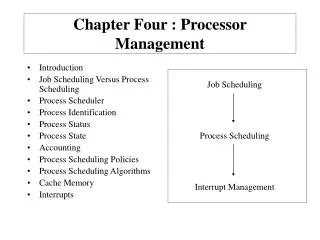
Scheduling Concepts CPU SCHEDULING Multiprogramming A number of programs can be in memory at the same time. Allows overlap of CPU and I/O. Jobs (batch) are programs that run without user interaction. User (time shared) are programs that may have user interaction. Process is the common name for both. CPU - I/O burst cycle Characterizes process execution, which alternates, between CPU and I/O activity. CPU times are generally much shorter than I/O times. Preemptive Scheduling An interrupt causes currently running process to give up the CPU and be replaced by another process. Blog: aforajayshahnirma.wordpress.com
The Scheduler CPU SCHEDULING • Selects from among the processes in memory that are ready to execute, and allocates the CPU to one of them • CPU scheduling decisions may take place when a process: 1. Switches from running to waiting state 2. Switches from running to ready state 3. Switches from waiting to ready 4. Terminates • Scheduling under 1 and 4 is nonpreemptive • All other scheduling is preemptive Blog: aforajayshahnirma.wordpress.com
The Dispatcher CPU SCHEDULING • Dispatcher module gives control of the CPU to the process selected by the short-term scheduler; this involves: • switching context • switching to user mode • jumping to the proper location in the user program to restart that program • Dispatch latency – time it takes for the dispatcher to stop one process and start another running Blog: aforajayshahnirma.wordpress.com
CPU SCHEDULING • Pre-emptive PRIORITY BASED SCHEDULING: • Assign each process a priority. Schedule highest priority first. All processes within same priority are FCFS. • Priority may be determined by user or by some default mechanism. The system may determine the priority based on memory requirements, time limits, or other resource usage. • Higher priority task can take control and after completion of higher priority task, it returns the control to lower priority task. Blog: aforajayshahnirma.wordpress.com
CPU SCHEDULING • Definitions: • Context Switch Changing the processor from running one task (or process) to another. Implies changing memory. • Reschedule latency How long it takes from when a process requests to run, until it finally gets control of the CPU. Blog: aforajayshahnirma.wordpress.com
Basic Diagram of context switching Process 2 Process 1 Scheduler Save content • Context= register+ data pointer + variable + stack area • When task switch occur, the context of interrupted task must be saved so that task can be continued properly when it receives next time slice. Blog: aforajayshahnirma.wordpress.com
MMX™ Technology • Multimedia Extensions (MMX) is a set of new instructions introduced to aid video and audio processing. • They perform single-instruction multiple data (SIMD) operations. • Perform parallel operations on packed integers in the floating point registers. • Floating point registers used for compatibility. Blog: aforajayshahnirma.wordpress.com
Hyper-Threading Technology • Enables a single physical processor to execute two separate code streams (threads) concurrently. • Each logical processor has its own set of registers. • Logical processors share the core resources of the physical processor including the execution engine and the system bus. Blog: aforajayshahnirma.wordpress.com
Hyper threading • A technology developed by Intel that enables multithreaded(current of data) software applications to execute threads in parallel on a single processor instead of processing threads in a linear fashion. Older systems took advantage of dual-processing threading in software by splitting(dividing) instructions into multiple streams so that more than one processor could act upon (on)them at once. Blog: aforajayshahnirma.wordpress.com
Why multicore? New modern processors are launched How to make a use of new technologies? Quad-core CPU Dual-core CPU 23 Blog: aforajayshahnirma.wordpress.com
Dual-core, Max. speedup ~2x Quad-core, Max. speedup ~4x Blog: aforajayshahnirma.wordpress.com 24
• Difficult to make single-core clock frequencies even higher • Deeply pipelined circuits(term): – heat problems • Many new applications are multithreaded • General(common) trend in computer architecture Blog: aforajayshahnirma.wordpress.com
• Editing a photo while recording a TV showthrough a digital video recorder • Downloading software while running ananti-virus program • “Anything that can be threaded today willmap efficiently to multi-core” Blog: aforajayshahnirma.wordpress.com
Summary • Multi-core chips animportant new trend incomputer architecture • Several new multi-corechips in design phaseslikely to gain importance Blog: aforajayshahnirma.wordpress.com
What is L1 and L2? • Level-1 and Level-2 caches • The cache memories in a computer • Much faster than RAM • L1 is built on the microprocessor chip itself. • L2 is a seperate chip • L2 cache is much larger than L1 cache Blog: aforajayshahnirma.wordpress.com
Tri core Phenom X3 Architecture Intel Core2Duo AMD Phenom Core 1 Core 2 Shared 4MB L2 Cache Memory Core 1 Core 2 Core 3 512KB L2 512KB L2 512KB L2 Shared 2MB L3 Cache Chipset Chipset VS HyperTransport™ technology DDR2 Memory Blog: aforajayshahnirma.wordpress.com
Hyper Threading • The operating system treats the processor as two processors instead of one. This increases the speed of the computer. • Pentium 4, Core i7, Core i5, Core i3(Processors Using Feature) Blog: aforajayshahnirma.wordpress.com
Hyper-Threading Technology • Enablessoftware to take advantage of task-level, orthread-level parallelism by providing multiple logical processors withina physical processor package. • The two logical processors each have a complete set of architecturalregisters while sharing one single physical processor's resources. By maintaining the architecture state of two processors, an HT Technologycapable processor looks like two processors to software, includingoperating system and application code. Blog: aforajayshahnirma.wordpress.com
Hyper-Threading Technology Figure 4. Comparison of an IA-32 Processor Supporting Hyper-Threading Technology and a Traditional Dual Processor System Blog: aforajayshahnirma.wordpress.com
Motivations for Virtual Memory • Use Physical DRAM as a Cache for the Disk • Address space of a process can exceed physical memory size • Sum of address spaces of multiple processes can exceed physical memory • Simplify Memory Management • Multiple processes resident in main memory. • Each process with its own address space • Only “active” code and data is actually in memory • Allocate more memory to process as needed. • Provide Protection • One process can’t interfere with another. • because they operate in different address spaces. • User process cannot access privileged information • different sections of address spaces have different permissions. Blog: aforajayshahnirma.wordpress.com
CPU C a c h e regs Levels in Memory Hierarchy cache virtual memory Memory disk 8 B 32 B 4 KB Register Cache Memory Disk Memory size: speed: $/Mbyte: line size: 32 B 1 ns 8 B 32 KB-4MB 2 ns $125/MB 32 B 1024 MB 30 ns $0.20/MB 4 KB 100 GB 8 ms $0.001/MB larger, slower, cheaper Blog: aforajayshahnirma.wordpress.com
Architectural Features of Core 2 • SSSE3 SIMD instructions • Intel Virtualization Technology, multiple OS support • LaGrande Technology, enhanced security hardware extensions • Execute Disable Bit • EIST (Enhanced Intel SpeedStep Technology) • Intel Wide Dynamic Execution • Intel Intelligent Power Capability • Intel Advanced Smart Cache • Intel Smart Memory Access • Intel Advanced Digital Media Boost Blog: aforajayshahnirma.wordpress.com
What is an instruction set? • All instructions, and all their variations, that a processor can execute • Types: • Arithmetic such as add and subtract • Logic instructions such as and, or, and not • Data instructions such as move, input, output, load, and store • Part of the computer architecture • Distinguished from the microarchitecture • Different microarchitectures can share common instruction set while their internal designs differ Fetch Decode Operand Fetch Execute Retire Blog: aforajayshahnirma.wordpress.com
VM • Address space is a set of mappings to data objects. • An address is only valid if it is mapped to an existing object • File system provides the name space and mechanisms to access data. • Uses the vnode layer to interact with the file system. • Each named memory object is associated with a vnode (but a vnode may map to many objects) • Unnamed objects represented by anonymous objects • Physical memory is treated as a cache for the data objects • Page is the smallest unit of allocation, protection, address translation and mapping. • Address space can be thought of as an array of pages Blog: aforajayshahnirma.wordpress.com
Due to increasing gap between CPU and main Memory, small SRAM memory called L1 cache inserted. • L1 caches can be accessed almost as fast as the registers, typically in 1 or 2 clock cycle • Due to even more increasing gap between CPU and main memory, Additional cache: L2 cache inserted between L1 cache and main memory : accessed in fewer clock cycles. Blog: aforajayshahnirma.wordpress.com
L2 cache attached to the memory bus or to its own cache bus • Some high performance systems also include additional L3 cache which sits between L2 and main memory . It has different arrangement but principle same. • The cache is placed both physically closer and logically closer to the CPU than the main memory. Blog: aforajayshahnirma.wordpress.com
Pentium Features • 64 bit data bus-allows 8 byte of data in a single bus cycle • Instruction cache-8kb,read only,32 bytes to be transferred from cache to buffer • Data cache-8kb,dual ported • 2 parallel integer execution unit-execution of 2 instruction in a single processor clock • Floating point unit-faster operation , dual processing support, interrupt controller Blog: aforajayshahnirma.wordpress.com
Pentium Features • Branch prediction logic-to reduce time required for branch caused by internal delay • Data integrity and error detection-data parity checking is done on byte by byte basis • Dual integer processor-allows execution of 2 instruction per clock cycle • Functional redundancy check-provide maximum error detection, 2nd processor [checker] samples master’s output and compares the values with internal computed values • Superscalar architecture-3 execution unit. 1 for floating point instruction and 2 U-V pipe for integer instruction. Capable of parallel execution of several instruction. Blog: aforajayshahnirma.wordpress.com
The Pentium CPU (MMX) Blog: aforajayshahnirma.wordpress.com
Pipelined Integer Unit As it can be seen from the previous diagram, the Integer unit has two pipelines(U and V),while the Floating Point Unit (FPU) has one pipeline. The Pentium pipelined Integer Unit supports 5 stages: 1) Pre-fetch 2) Decode 3) Address generate 4) EX Execute - ALU and Cache Access 5) WB Write back Although different later processors like the MMX tampered with the 5 execution steps(by adding intermediate LIFO structures to hold bulks of instructions), the steps remain the core foundation of the pipelining. Blog: aforajayshahnirma.wordpress.com
Pipelined Integer Unit In the Pre-fetch cycle, two pre-fetch buffers read instructions to be executed. Instructions can be fetched from the U or V pipeline. The U pipeline contains more complex instructions. 2) In the Decode cycle, two decoders, decode the instructions and try to pair them together so they can run in parallel , since the Pentium features a Superscalar architecture. Even though the Pentium processor features a Superscalar architecture, in order for two instructions to run concurrently, like in the diagram below, they need to satisfy some rules. Essentially, the instructions have to be independent otherwise they cannot be paired together. 3) In the second Decode stage, or the address generate stage, the addresses of memory operands are calculated. After these calculations, the EX stage of the pipeline is ready to execute. A Floating Point instruction cannot be paired with an Integer instruction. Blog: aforajayshahnirma.wordpress.com
Pipelined Integer Unit (Conclusion) 4) In the Execution cycle, the ALU is reached. 5) In the Write Back cycle, information is written back to the registers. For two instructions to be paired together in the Decode stage, they have to lack dependencies.The two paired instructions would also have to be basic, in the sense that they contain no displacements or immediate addressing. As it can be deduced, pipelines will sometimes execute an instruction at the time, despite the Superscalar ability. If two instructions are executing concurrently in the pipeline (given they satisfy the proper conditions, and are independent) and one of them stalls as a result of hazard control, the other one will also stall. Blog: aforajayshahnirma.wordpress.com
Branch Prediction Other than the Superscalar ability of the Pentium processor, the branch prediction mechanism is a much-debated improvement. Predicting the behaviors of branches can have a very strong impact on the performance of a machine. Since a wrong prediction would result in a flush of the pipes and wasted cycles. The branch prediction mechanism is done through a branch target buffer. The branch target buffer contains the information about all branches. The prediction of whether a jump will occur or no, is based on the branch’s previous behavior. There are four possible states that depict a branch’s disposition to jump: Stage 0: Very unlikely a jump will occurStage 1: Unlikely a jump will occurStage 2: Likely a jump will occurStage 3: Very likely a jump will occur Blog: aforajayshahnirma.wordpress.com
Branch Prediction When a branch has its address in the branch target buffer, its behavior is tracked. This diagram portrays the four stages associated branch prediction. If a branch doesn’t jump two times in a row, it will go down to State 0. Once in Stage 0, the algorithm won’t predict another jump unless the branch will jump for two consecutive jumps (so it will go from State 0 to State 2) Once in Stage 3, the algorithm won’t predict another no jump unless the branch is not taken for two consecutive times. Blog: aforajayshahnirma.wordpress.com
Branch Prediction It is actually believed that Pentium’s algorithm for branch prediction is incorrect. As it can be seen in the diagram to the right, State 0 will jump directly to State 3, instead of following the usual path which would include State 1, and State 2. This abnormality might be attributed to the way in which the branch target buffer operates: • If a branch is not found in the branch target buffer, then it predicted that it won’t jump.- A branch won’t get an actual entry in the branch target buffer, until the first time it jumps, and when it does, it goes straight into State. - Because the branch won’t get an entry into the branch target buffer until the first time it jumps, this will cause an alteration into the actual state diagram, as it can be clearly seen. Blog: aforajayshahnirma.wordpress.com
Branch Prediction (in later Pentium Models) The Intel Pentium branch prediction algorithm is indeed better than a 50% guess, but it has limitations. In a need to increase the accuracy of branch predictions, the processors following the Pentium adopted a different branch prediction algorithm. Some loops have repetitive patterns and they need to be recognized. With a two bit binary counter, it is impossible to attain any complexity. Later generation processors, such as the Pentium MMX, Pentium Pro, Pentium II, use another mechanism for branch prediction. A 4 bit register is used to record the previous behavior of the branch. If the 4 bit register would be 0001, it would mean that the branch only jumped the last time out of 4. A 4 bit register would not be of much use without any additional logic. In addition to the 4 bit register, there are 16, 2-bit counters like the ones that were previously shown. Blog: aforajayshahnirma.wordpress.com