Download
1 / 27
270 likes | 378 Views
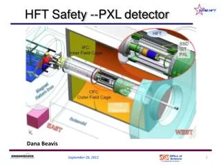
HFT PIXEL Detector WBS 1.2. Howard Wieman LBNL. Topics - PXL (WBS 1.2). PXL design and status Deliverables Development and Construction Plan Schedule Risks Cost Manpower. Pixel geometry. These inner two layers provide the projection precision. End view. 8 cm radius. 20 cm.

E N D
HFT PIXEL DetectorWBS 1.2 Howard Wieman LBNL
Topics - PXL (WBS 1.2) • PXL design and status • Deliverables • Development and Construction Plan • Schedule • Risks • Cost • Manpower
Pixel geometry. These inner two layers provide the projection precision End view 8 cm radius 20 cm 2.5 cm radius Inner layer Outer layer coverage +-1 One of two half cylinders total 40 ladders
Some pixel features and specifications critical and difficult more than a factor of 3 better than other vertex detectors (ATLAS, ALICE and PHENIX)
Performance features pointing accuracy comparison Hybrid uncertainty area -------------------------------- MAPS uncertainty area • 50 m Silicon detector chips, MAPS • thin • small pixels, high resolution • Air cooling • Mechanical stability
Alternate Technologies Considered • Hybrid • X0 large (1.2%) • Pixel Size large (50 m x 450 m) • Specialized manufacturing - not readily available • CCDs • Limited radiation tolerance • Slow frame rate, pileup issues • Specialized manufacturing • DEPFET • Specialized manufacturing • very aggressive unproven technology
The detector ladders are thinned silicon, on a flex kapton/aluminum cable The large CTE difference between silicon and kapton is a potential source of thermal induced deformation even with modest 10-15 deg C temperature swings Two methods of control ALICE style carbon composite sector support beam with large moment of inertia Soft decoupling adhesive bonding ladder layers Stability requirement drives design choices
HFT PXL status • Mechanical stability analysis completed (controlled to 20 m) • thermal deformation • gravity induced sag • humidity induced deformation • support vibration
HFT PXL status-thermal analysis and testing • Silicon power: 100 raised to 170 mW/cm2 (~ power of sunlight) • 350 W total Si + drivers
PXL status - thermal test results max min Hot spots for images at location 0-21 cm (3 cm step): 41.2, 42.5, 41.4, 41.6, 41.4, 40.5, 40.1, 38.3 ºC room “sensor” heaters: ~230 W Pt heaters: ~25 W Driver heaters: ~40 W Total: ~295 W Airflow 16 m/s ∆T above ambient room temperature: 11.5 deg C
3 µm 3 µm 2 µm 8 µm 4 µm 11 µm HFT PXL status – air flow vibration tests carbon fiber sector beam capacitance vibration probe two positions shown air in air out adjustable wall for air turn around reinforced end no reinforcement at the end air velocity probe two positions shown
HFT PXL status – insertion design insertion mechanism to guide detector around beam pipe and beam pipe support uses track and carriage with hinge and cam to guide into final docking position
HFT PXL status – installation design • a well controlled method for installation of the pixel detector has been developed with emphasis on ease of operation and avoidance of detector risk • The PXL assembly will be enclosed in a carrying box that is equipped for transfer of the detector assembly into the PXL support tube • Once inserted on tracks the detector is guided into position locking kinematic mounts
PXL Deliverables • Pixel Insertion Structure • Pixel Insertion Tool • a total of 10 sectors, with each sector containing: • one ladder at a radius of 2.5 cm • three ladders at a radius of 8.0 cm • With each ladder containing: • ten Si detector elements • one readout board • two DAQ receiver PCs • PC based control and monitoring system • two clam shells, with 5 sectors integrated and aligned on each clam shell • The two clam shells will be installed in Pixel Insertion Tools, ready for insertion onto the New Cone Structure • One additional complete detector and sufficient sector and populated ladder components to have the capability to fabricate two more complete detector assemblies • Provide services including cabling and cooling
PXL WBS items (high level) • 1.2.1 PXL Mechanics • 1.2.1.1 Module Support (Sector) • 1.2.1.2 Detector Support (D-Tube/Kinematic Mount) • 1.2.1.3 Insertion Mechanism and Internal Service Support • 1.2.2 PXL Electronics • 1.2.2.1 Phase-1 PXL Sensor Chips • 1.2.2.2 Final PXL Sensor Chips • 1.2.2.3 Ladder Cable • 1.2.2.4 PXL Prototype Ladder Assembly • 1.2.2.5 Read-Out Electronics • 1.2.2.6 PXL Sensor Ladder Production • 1.2.3 Detector Assembly • 1.2.3.1 Prototype Sector Assembly • 1.2.3.2 D-Tube Assembly and Survey Tool (Engineering) • 1.2.3.3 Sector Mount and Survey (Engineering) • 1.2.3.4 Final Assembly (Engineering) • 1.2.3.5 Production Sector Assembly • 1.2.3.6 D-Tube Assembly • 1.2.3.7 Sector Mount and Survey • 1.2.3.8 Final Assembly (Production) • 1.2.3.9 System Test (Production) • 1.2.4 Infrastructure • 1.2.4.1 Cables • 1.2.4.2 Cooling Services • 1.2.4.3 Rack Equipment • 1.2.5 Installation • 1.2.5.1 Pixel Installation in-situ
Electronics Development Plan • Develop sensor chips, 3 generation program (WBS 1.2.2.2) • Develop readout electronics (WBS 1.2.2.5) • STAR compatible readout system - limited channel count • Upgrade to full detector capability • Develop flex PC readout cable (WBS 1.2.2.3) • copper version • aluminum version • Develop chip testing and characterization system (WBS 1.2.2.5, 1.2.2.6) • chip level • probe test level • Production testing of ladders (WBS 1.2.2.6)
Mechanical Development plan • Design detector structures (WBS 1.2.1.1, 1.2.1.2, 1.2.3) • Design fabrication tooling (WBS 1.2.1.1, 1.2.3) • Design installation (WBS 1.2.1.3, 1.2.5) • Analyze structure stability and cooling (WBS 1.2.1.3) • Prototype structures using developed tooling (WBS 1.2.1.1,1.2.1.2, 1.2.1.3) • Test structure stability and cooling (WBS 1.2.1.1,1.2.1.2, 1.2.1.3) • Prototype installation and insertion (WBS 1.2.1.2, 1.2.1.3) • Prototype sectors with prototype sensors (WBS 1.2.1.1, 1.2.1.2) • Design and build cooling plant (WBS 1.2.4.2) • Test engineering prototype • Install and operate engineering prototype (WBS 1.2.5) • Produce final detector sectors (WBS 1.2.3.8) • Test final detector system (WBS 1.2.3.9) • Install and operate final detector system (WBS 1.2.5)
Summary • MAPS technology development going well • Readout electronics well advanced and tested • Very low mass detector support designs have passed multiple analysis tests and prototype tests addressing cooling and position stability. • Tooling is in place and tested for sector/ladder production • Concept designs for installation and insertion are well advanced • Risks have been identified and are being addressed at an early stage • Design and testing have matured sufficiently to make accurate cost estimates
Mimostar–2 30 µm pixel, 128 x 128 array 1.7 ms integration time 1 analog output Mimostar–3 30 µm pixel, 320 x 640 array 2.0 ms integration time 2 analog outputs Phase–1 30 µm pixel, 640 x 640 array 640 µs integration time, CDS 4 binary digital outputs Final (Ultimate) 18.4 µm pixel, 1024 x 1088 array ≤ 200 µs integration time, CDS, zero suppression 2 digital outputs (addresses) Sensor and Readout Development Plan Gen Sensor Sensor RDO 50 MHz readout clock JTAG interface, control infrastructure ADCs, FPGA CDS & cluster finding zero suppression ≤ 4 sensor simultaneous readout 160 MHz readout clock JTAG interface, control infrastructure zero suppression 120 sensor simultaneous readout 160 MHz readout clock JTAG interface, control infrastructure 400 sensor simultaneous readout (full system) 1 DONE 1 2 PROTOTYPED 3