Download
1 / 36
360 likes | 513 Views
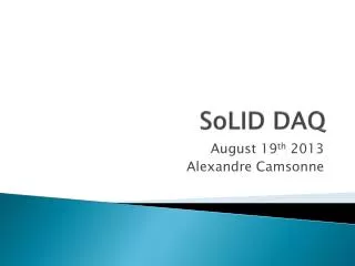
DAQ Hardware Status 9 September 2008 Matt Warren Valeria Bartsch, Veronique Boisvert Maurice Goodrick, Barry Green, Bart Hommels, Marc Kelly, Andrzej Misiejuk, Vishal Panchal, Martin Postranecky, Tao Wu. DIF. DIF. DIF. DIF. Detector Unit. Detector Unit. Detector Unit. Detector Unit.

E N D
DAQ Hardware Status9 September 2008Matt WarrenValeria Bartsch, Veronique BoisvertMaurice Goodrick, Barry Green, Bart Hommels, Marc Kelly, Andrzej Misiejuk, Vishal Panchal, Martin Postranecky, Tao Wu
DIF DIF DIF DIF Detector Unit Detector Unit Detector Unit Detector Unit Storage DAQ architecture Detector Unit: ASICs DIF: Detector InterFace connects Generic DAQ and services LDA: Link/Data Aggregator – fanout/in DIFs and drives link to ODR ODR: Off Detector Receiver – PC interface for system. CCC: Clock & Control Card: Fanout to ODRs (or LDAs) CONTROL PC: DOOCS GUI (run-control) NEW! DAQ PC ODR LDA Control PC (DOOCS) CCC LDA DAQ PC ODR Matt Warren et al. - DAQ Status - CALICE Manchester
CCC Matt Warren et al. - DAQ Status - CALICE Manchester
Overview Schematic CLOCK Fanout Prog. Delay 64*.5ns CPLD Fanout D CONTROLS (TRAINSYNC) 8x HDMI SPARE FAST_OUT (TRIGGER) Fanout FAST_IN (BUSY) Matt Warren et al. - DAQ Status - CALICE Manchester
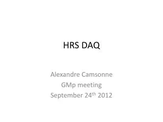
Detailed Overview Schematic • NOTES: • CPLD + Gates • Busy == Gen • Added SPARE line • Delayed clock option • 4x 8 way DIL to CPLD CLOCK AUTO/ XTAL SW LVDS on SMA LVTTL on Lemo 8x LVDS on HDMI MPX +PLL NIM/TTL on Lemo 8x LVDS on SMA 2x LVTTL on Lemo ~50 MHz 2x NIM on Lemo X-TAL ASYNC clock LVDS on SMA SW 8x LVDS on HDMI ECL on 2pin Lemo DELAY Controls (SYNCCMD, BUSY-IN etc) 4x LVDS on SMA 4x NIM on Lemo 4x 4 SW-2 5->1 4 8x LVDS on HDMI GEN (was BUSY) LVDS on SMA CPLD (Xilinx Coolrunner XCR3128XL-7) SW-3 2->1 8x LVDS on HDMI NIM on Lemo 4 o/c TTL on Lemo SPARE (DATA_D2L) 8x LVDS on HDMI LVTTL on Lemo RS232 DEBUG 4x 8way DIL PCB Header Matt Warren et al. - DAQ Status - CALICE Manchester
C&C Logic and Interfaces CPLD (XCR3128XL-7) replacing many jumpers and switch logic RS232 interface as a means of control Many buffers, 0Ω resistors and solder links for better signal integrity, isolation and configuration Signal Inputs: • CLOCK • 1x LVDS (SMA DC) • 1x LVTTL DC (Lemo) • 1x NIM/TTL (Lemo) AC/DC • ASYNC • LVDS (SMA) DC • ECL (2 pin LEMO) AC • Controls (SYNCCMD, BUSY etc. + more) • 4x LVDS (SMA) • 4x NIM/TTL (Lemo) AC/DC Signal Outputs: • CLOCK • 2x LVTTL on Lemo • 2x NIM on Lemo • 2x LVDS on SMA • 8x LVDS on DIL Header • TRAINSYNC • LVTTL on Lemo • GEN (was Busy) • LVDS on SMA • NIM on Lemo • OC-TTL on Lemo • Spare (DATA_D2L) • LVTTL on Lemo • HDMI I/O: x8 • - LVDS AC/DC • OUT: • CLOCK • ASYNC • TRAINSYNC • IN: • GEN (was BUSY) • SPARE(DATA_D2L) *NO RJ45 Matt Warren et al. - DAQ Status - CALICE Manchester
Some Hardware Details • Clock: • PLL/MUX - ICS581-02 • +/-150 ps jitter • 45min/55max Duty Cycle • Failover if external clock missing for 3 cycles. • Local Osc. 100 MHz/2 = 50% duty-cycle 50MHz • CPLD: Xilinx CoolRunner XPLA3 XCR3128XL-7 • 3.3V, low power • 128 macrocells with 3,000 usable gates • 5.5ns pin-to-pin logic delays • Extra IO via IDC header. • Single PCB with connectors at the edge (big!) • Separate PSU • Clock Delay Option to CPLD – 64x0.5ns • For signal deskew (CLOCK unaffected) Matt Warren et al. - DAQ Status - CALICE Manchester
Board Layout SMAs (vertical) HDMIs LEMO (NIM) Eurocard size (234x220mm) CPLD Debug Header RS232 Add-ons interface Matt Warren et al. - DAQ Status - CALICE Manchester
Status/Schedule • Schematic DONE. • Layout DONE. • Manufacture IN PROGRESS . • Started last week (1 Sept). • Run of 2 with 8 more when satisfied working • Manufacturing PCBs for all 10 (2x price = 10x price!) • Will do second run of PCBs if any problems found • First 2 boards due week of 15 Sept, BUT component lead-times may delay a few weeks. • Next 8 loaded as soon as testing is complete. • Procured components for all 10 now, so won’t delay further. • Next: Firmware development! Matt Warren et al. - DAQ Status - CALICE Manchester
CCC Link Signals CLOCK Machine clock (50-100MHz) TRAINSYNC_OUT Synchronisation of all the front-end slow clocks. An external signal will be synchronized with/to CLOCK, phase adjusted and transmitted as a single clock-period wide pulse to the LDA. To allow communicating with a stand-alone DIF, the CCC board will can be configured to send the LDA 8b/10b serialised command for train-sync. FAST_OUT Transfer asynchronous triggers as fast as possible. In AUTO mode, used to Transfer BUSY to detector (toggle = level) FAST_IN Used by DIFs (via LDA) signal to “stop acquisition” when needed. Due to AC coupling the busy must asserted by constantly toggling this line. Uses same HDMI cable and signal types/direction Matt Warren et al. - DAQ Status - CALICE Manchester
Timing Overview • Presume machine CLOCK period < bunch-period • Expected to be 50-100MHz, local or machine. • Common fanned-out to the detector • BUNCH-CLOCK (slow clock) derived as CLOCK/n • Re-produced locally on DIF (with TRAINSYNC & counter) • Start of train signal (TRAINSYNC) synchronises bunch-clocks on all DIFs. • Requires fixed-latency signal – a SYNCCMD. • TRAINSYNC “qualifies” CLOCK edge CLOCK BUNCH-CLOCK TRAIN-SYNC Matt Warren et al. - DAQ Status - CALICE Manchester
SYNCCMD Details • SYNCCMD is the ONLY mechanism for synchronising DIFs • 4 (or 16) types of command are possible. • Expects a PRE bunch-train/spill signal • Signal in known phase with BUNCH CLOCK • Fixed period prior to first bunch of train • Synchronous to CLOCK • CCC card forwards signal to LDAs • Synchronises signal to local clock when needed • LDA stores arrival time wrt serialiser bit counter. • Next Word to DIFs replaced with special SYNCCMD word • First byte dedicated K character • Second byte (7:6): Type; (5:0): Delay (could be 3:5 ratio too) • SYNCCMD system on DIF delays signal specified number of CLOCKs and issues the required signal. Data 15:8 Data 7:0 KSYNCCMD 0:8 Data 15:8 Data 7:0 0 1 2 3 4 5 6 7 8 9 10 11 12 13 14 15 16 17 18 19 0 1 2 3 4 5 6 7 8 9 10 11 12 13 14 15 16 17 18 19 LDA In DIF Out Matt Warren et al. - DAQ Status - CALICE Manchester
(generic) DIF Matt Warren et al. - DAQ Status - CALICE Manchester
DIF HDMI cable pseudo-LDA AC-coupling adapter DIF -LDA link testing • Link shows signs of life. • pseudo-LDA sends CLK & 8B/10B data @ 100MHz over AC-coupled LVDS on HDMI cables data loop-back in firmware stable Matt Warren et al. - DAQ Status - CALICE Manchester
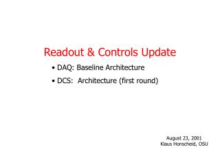
DIF: Status (generic) and Plans ECAL DIF prototype: 65x72mm, 8 layers • JTAG programming header • LDA link HMDI connector • DIF link connector • mini-USB connector • Xilinx PROM • Cypress 2MB 10ns SRAM • Xilinx Spartan3-1000 FPGA • FDTI FT245R USB controller • 20p user header connector • reset pushbutton • 90pin SAMTEC IB connector e.g: ECAL DIF • Test hardware in place • Firmware development started • LDA Link integration • 2 DIFs produced, parts available for 10 more. • DIF hardware is (at least partly) functional Matt Warren et al. - DAQ Status - CALICE Manchester
LDA Matt Warren et al. - DAQ Status - CALICE Manchester
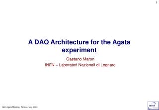
LDA-ODR Connectivity • Prototype LDA has hardware problems. • Mainly incorrect signals routed on PCB to Eth add-on • LDA has been modified to attempt fix (see pic!) • Ethernet RX OK, auto-negotiation starts OK. BUT .. • Ethernet TX appears corrupt • random glitches and/or clock recovery problems. • PHY in loop-back OK, so looks like the SERDES • Investigating … • SOME GOOD NEWS: • ODR-LDA protocol almost finalised Matt Warren et al. - DAQ Status - CALICE Manchester
LDA-DIF Connectivity • Current boards have 8 working HDMI links, • Option for 10 on future boards with simple change of FPGA. • FPGA is basically used as an LVDS transceiver and clock fanout, although it will probably also handle the separate prompt/fast signals to/from the DIF. • Link documentation is proceeding, large amounts have been already done. Matt Warren et al. - DAQ Status - CALICE Manchester
New LDA Base Board • Enterpoint is designing a replacement board for the BroadDown2 known as the Mulldonoch2. • Extra I/O capabilities. • EBX format board. • PCI connector is replaced by a PC104 connector. • SDRAM onboard. • SPI flash ram. • Better power system • Prototype production is expected sometime this month. • Is not designed for us especially, but rather is a generic board Enterpoint had planned already. Design time table got shifted when we found the error in the existing BD2 design. • A corrected BroadDown2 design is also going to be available in roughly the same time frame. Matt Warren et al. - DAQ Status - CALICE Manchester
LDA: Conclusions • Need to get Ethernet working, without that we are dead in the water currently. • Then we can proceeded with more of the firmware development and begin to get to a point where it might actually be useful and talk to the outside world. • Need to consider what the BD2->MD2 migration path means for us, with regard to possible changes to LDA design, to include more features etc. • Possible re-spin of the Ethernet Board, to remove the bits we don't want/need and lower cost of it. ( MD2 might already have USB built in, and we might decide to skip the TLK2501 all together). • Possible extra HDMI interface expansion given the extra IO. • Bench tests need to be done on the timing/synchronisation system to make sure we can achieve in practice what we thought was possible. Matt Warren et al. - DAQ Status - CALICE Manchester
ODR Matt Warren et al. - DAQ Status - CALICE Manchester
Hardware/Firmware • ODR is working(!) • Receive data on 4x fibre (RX), • Write to disk FAST (250MB) • Send data up fibre (TX) • Controlled from Linux driver • Future upgrade: Decode event header from LDA • Provides on-line info • Can deal with control messages from LDA • Allows host to write to disk without processing Matt Warren et al. - DAQ Status - CALICE Manchester
Rate performance optimization (from ODR to disk) • Several factors to optimize: • Architecture of the host (hyper-threading, raid array disks, kernel version, etc) • Number of DMA buffers • currently using 950 • Number of buffers to fill before dumping the data to disk • best to have about N DMA buffers - 200 (so 750 for 950 DMA buffers) • Size of files to write (grouping of data files) • Called dumpdatasize on plot • Dominant factor • chose 100 MB 1 MB 1 channel, writing to raid 200 MB V. Panchal, V. Boisvert, A. Misiejuk Matt Warren et al. - DAQ Status - CALICE Manchester
Supervisor ODR VHDL code FIFO Dup. DOOCS Interface Data Buff Data Buff Data Buff Software: Interface to DOOCs DOOCS TX LDA msg Config/TX DMA FIFO to user buffer Two way communication Requester DMA data to user buffer(s) (host memory) Hardware ODR Software ODR Matt Warren et al. - DAQ Status - CALICE Manchester
Demo Construction (Advert!) Control Room PC DOOCS GUI laptop DAQ PC caldaq1 LDA Emulator PC ldaemu1 ODR Gbit Fibre NIC RAID Storage ODR Driver DOOCS Hardware Interface Network Switch Cu NIC • Control PC signals LDA Emulator (via ODR) to start or stop sending data with command messages • ODR receives data and writes it to disk. Matt Warren et al. - DAQ Status - CALICE Manchester
The End Matt Warren et al. - DAQ Status - CALICE Manchester
(actually not the end) Extra slides on C+C Matt Warren et al. - DAQ Status - CALICE Manchester
Introduction • Goal: A timing system compatible with everyone (Remi/Vincent/Mathias etc. been asking good questions) • Looked at details of: • Operating modes • Trigger • Auto • Single • Machine interface/sync • Synchronisation of detector • Signalling over our cables • Common usage AND SIGNAL NAMING • Handing FE errors etc (BUSY) Matt Warren et al. - DAQ Status - CALICE Manchester
Connection Overview 1 Control PC 1 CCC 8 LDA 8 DIFs DIF DIF DIF DIF DIF DIF x8 LDA LDA LDA x8 Control Room PC CCC Matt Warren et al. - DAQ Status - CALICE Manchester
Timing Overview • Presume machine CLOCK period < bunch-period • Expected to be 50-100MHz, local or machine. • Common fanned-out to the detector • BUNCH-CLOCK (slow clock) derived as CLOCK/n • Re-produced locally on DIF (with TRAINSYNC & counter) • Start of train signal (TRAINSYNC) synchronises bunch-clocks on all DIFs. • Requires fixed-latency signal – a SYNCCMD. • TRAINSYNC “qualifies” CLOCK edge CLOCK BUNCH-CLOCK TRAIN-SYNC Matt Warren et al. - DAQ Status - CALICE Manchester
SYNCCMD Details • SYNCCMD is the ONLY mechanism for synchronising DIFs • 4 (or 16) types of command are possible. • Expects a PRE bunch-train/spill signal • Signal in known phase with BUNCH CLOCK • Fixed period prior to first bunch of train • Synchronous to CLOCK • CCC card forwards signal to LDAs • Synchronises signal to local clock when needed • LDA stores arrival time wrt serialiser bit counter. • Next Word to DIFs replaced with special SYNCCMD word • First byte dedicated K character • Second byte (7:6): Type; (5:0): Delay (could be 3:5 ratio too) • SYNCCMD system on DIF delays signal specified number of CLOCKs and issues the required signal. Data 15:8 Data 7:0 KSYNCCMD 0:8 Data 15:8 Data 7:0 0 1 2 3 4 5 6 7 8 9 10 11 12 13 14 15 16 17 18 19 0 1 2 3 4 5 6 7 8 9 10 11 12 13 14 15 16 17 18 19 LDA In DIF Out Matt Warren et al. - DAQ Status - CALICE Manchester
Timing Environment • CCC does NOT support varied delays on individual outputs. • LDAs can NOT adjust individual link timings • Presumed cables to all LDAs equal length • DIFs need to adjust own timing if needed • FPGA resources (or board) • Custom cables (available?) • CCC card can adjust timing of TRAINSYNC wrt CLOCK (1/2 ns steps) Matt Warren et al. - DAQ Status - CALICE Manchester
CCC Link Interface • CCC connects to LDA, DIF and ODR using the ‘standard’ HDMI cabling and connectors and pinout (CLink) • CCC can be used as a pseudo-LDA for stand-alone DIF testing • A distinction is made between fast and fixed latency signals: • Fast signaling is asynchronous and uses a dedicated line to transfer a pulse. No attempt is made to encode data. • Fixed-latency signaling will not arrive fast, but will arrive a known latency after reception by CCC (Jitter 1 CLOCK). Matt Warren et al. - DAQ Status - CALICE Manchester
Detector Operating Modes • Triggered • External signal causes ASICs to take data • Single (auto-trig) • ASICs auto select data, but readout controlled by trigger • Burst (auto-trig) • ASICs signal when full • Fed to CCC as BUSY • CCC sends stop-acquisition signal to entire detector Remi Cornat Matt Warren et al. - DAQ Status - CALICE Manchester
CCC Link Signals CLOCK Machine clock (50-100MHz) TRAINSYNC_OUT Synchronisation of all the front-end slow clocks. An external signal will be synchronized with/to CLOCK, phase adjusted and transmitted as a single clock-period wide pulse to the LDA. To allow communicating with a stand-alone DIF, the CCC board will can be configured to send the LDA 8b/10b serialised command for train-sync. FAST_OUT Transfer asynchronous triggers as fast as possible. In AUTO mode, used to Transfer BUSY to detector (toggle = level) FAST_IN Used by DIFs (via LDA) signal to “stop acquisition” when needed. Due to AC coupling the busy must asserted by constantly toggling this line. Matt Warren et al. - DAQ Status - CALICE Manchester
Busy Flow DIF DIF DIF DIF GEN_D2L ASYNC_L2D LDA FAST_IN BUSY FAST_OUT STOP_AQU CCC Matt Warren et al. - DAQ Status - CALICE Manchester