Download
1 / 17
190 likes | 711 Views
FPGA. Sistemi Elettronici Programmabili. FPGA: Architettura. FPGA: Logic Element (Block). FPGA: LUT – Look Up Table (2 Ingressi). NOTA

E N D
FPGA Sistemi Elettronici Programmabili Sistemi Elettronici Programmabili
FPGA: Architettura Sistemi Elettronici Programmabili
FPGA: Logic Element (Block) Sistemi Elettronici Programmabili
FPGA: LUT – Look Up Table (2 Ingressi) Sistemi Elettronici Programmabili
NOTA L’esempio è una LUT a due ingressi e quattro bit di memoria. In ogni cella di memoria si può inserire il valore di una funzione di 2 bit – OR, AND, NOR, NAND, XOR, …- in funzione degli ingressi. Al momento del funzionamento IN [0,1] sceglie la cella di memoria – i quattro FF D – corrispondenti alla funzione desiderata FPGA LUT 2 INGRESSI Sistemi Elettronici Programmabili
FPGA: Programmazione Sistemi Elettronici Programmabili
FPGA: Programmazione (2) Sistemi Elettronici Programmabili
FPGA: LUT Sistemi Elettronici Programmabili
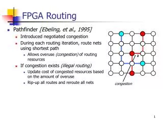
FPGA: Routing (VRC) Sistemi Elettronici Programmabili
FPGA: Routing (IM) Sistemi Elettronici Programmabili
FPGA: Programmazione (2) Sistemi Elettronici Programmabili
FPGA: Market SRAM Based Fuse Based Sistemi Elettronici Programmabili
FPGA: Logic Element (Block) - ALTERA Sistemi Elettronici Programmabili
ALTERA – Stratix: Architecture Sistemi Elettronici Programmabili
10 LEs per Logic Array Block (LAB) Local Interconnect Drives LE Inputs LAB-Wide Control Signals Stratix: Logic Array Blocks Control Signals 4 LogicElement LE1 4 LE2 4 LE3 4 LE4 Logic ArrayBlock 4 LE5 4 LE6 4 LE7 4 LE8 4 LocalInterconnect LE9 4 LE10 Sistemi Elettronici Programmabili
FPGA: Progettazione Library Block Diagram IP SM Simulazione Descrizione HDL Hardware Model Simulazione Sintesi Hardware Model Place & Route Simulazione Configuration Sistemi Elettronici Programmabili
FPGA: Programmazione (3) FPGA JTAG Adapter Data FPGA Configuration Device CTRL Data ADD Decoder μC RAM FPGA Sistemi Elettronici Programmabili