Download
1 / 1
10 likes | 106 Views
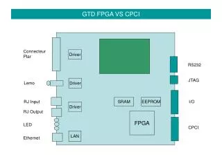
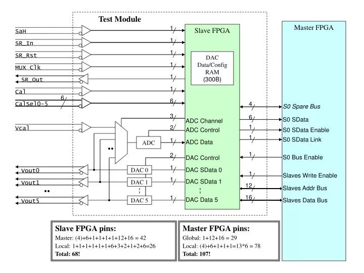
DAC 0. DAC 1. DAC 5. Test Module. Master FPGA. 1. Slave FPGA. SaH. 1. SR_In. 1. SR_Rst. DAC Data/Config RAM (300B). 1. MUX Clk. 1. SR_Out. 1. Cal. 6. 6. 4. CalSel0-5. S0 Spare Bus. 3. 6. S0 SData. ADC Channel. 1. 2. Vcal. ADC Control. S0 SData Enable. 1.

E N D
DAC 0 DAC 1 DAC 5 Test Module Master FPGA 1 Slave FPGA SaH 1 SR_In 1 SR_Rst DAC Data/Config RAM (300B) 1 MUX Clk 1 SR_Out 1 Cal 6 6 4 CalSel0-5 S0 Spare Bus 3 6 S0 SData ADC Channel 1 2 Vcal ADC Control S0 SData Enable 1 1 ADC S0 SData Link ADC Data 1 2 S0 Bus Enable DAC Control 1 Vout0 DAC SData 0 1 Slaves Write Enable 1 DAC SData 1 Vout1 12 Slaves Addr Bus 16 1 DAC Data 5 Vout5 Slaves Data Bus Slave FPGA pins: Master: (4)+6+1+1+1+1+12+16 = 42 Local: 1+1+1+1+1+1+6+3+2+1+2+6=26 Total: 68! Master FPGA pins: Global: 1+12+16 = 29 Local: (4)+6+1+1+1=13*6 = 78 Total: 107!