Download
1 / 58
580 likes | 741 Views
The CBM- MVD read -out system. Christoph Schrader for the CBM-MVD Collaboration. DAQ project p hases. Demo (MI20) data synchronization …. 2009 2010 2011 2012 2013 2014. Prototype v1 (MI26) conservative approach (based on LVDS signals) full readout concept

E N D
The CBM-MVDread-out system Christoph Schrader forthe CBM-MVD Collaboration
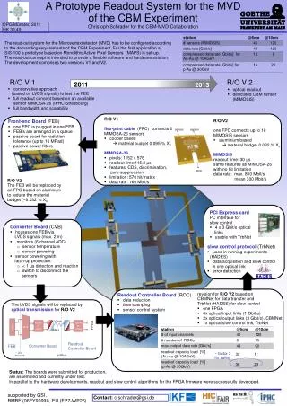
DAQ projectphases Demo (MI20) data synchronization … 2009 2010 2011 2012 2013 2014 • Prototype v1 (MI26) • conservative approach • (based on LVDS signals) • full readout concept • full bandwidth • Prototype v2 (MI26) • optical readout • sensor ladder • compatible to a dedicated MVD sensor Prototype SIS-100 (MISTRAL)
Prototype • Version 1
MIMOSA-26 9 hits/ row available ∑ 570 hits pixel array: 1152 columns x 576 rows (18.4 µm pitch and 115.2 µs readout time) DACs 4 x memorybanks multiplexer CDS 1152 discriminators zerosuppressionlogic Discri test Temp probe PLL JTAG Digital input Digital output Power 80 MHz 2 channels D0,D1+clock • ~ 80 Mbit/s (570 words of 16 bit • ~ 9120 bit/frame) 160 Mbit/s
Prototype Version1 sensors based on MIMOSA-26 vacuum clock start reset JTAG FPC FPC FPC FEB FEB FEB driver board . . . LVDS, 1m 4x 80 Mbit/s (MIMOSA-26) converter board converter board converter board . . . LVDS 4x 80 Mbit/s readout controller board readout controller board Slow control board . . . 2 Gbit/s optical fiber to the MVD network
Flex-Print Cable µm wire bonds 12.5 polyimide connector pads Adhesive (20 µm) 15 µm 18 copper/ aluminum 20 polyimide 50 sensor 25 10 ∑Cu~0.0861 % x/Xo* ∑Alu~0.032 % x/Xo *** * 100% fillfactor ** same dimensionascopper
Flex-Print Cable Single-ended crosstalk - 22 dB 10 MHz B. Neuman
Flex-Print Cable could be better to have differential signal for JTAG - 22 dB B. Neuman
FEB FPC FPC FPC FEB FEB FEB clock start reset JTAG FPC FPC . . . D0,D1 clock TDO Temp current FPC • The FEB: • transfer D0,D1,clock to • the converter boards (0.5 m away) • to loop clock, reset, start, JTAG • passive filters for power supply full passive board (more radiation tolerant)
Converter Board • signal conditioning for • data transfer • power supply for LVDS drivers • diodebasedtemperaturemeasurement (internalsensordiode) • 6 channelADCstotransfer in serial • thecurrentandtemperature • current monitor and protection to • disable the power of the sensors • (in case of latch-up) • switch for JTAGchain shutdown <2 µs FEB FEB FEB readout controller power on 200 µs converter board converter board converter board readout controller • seetalk: • M.Koziel
Sensor slow control via JTAG • Requirements for the slow control system: • Initializing of each sensor via JTAG • Scalability: >100 MAPS • Sequential reading of the sensor ID • Triggered monitoring/reprogramming of the sensor parameters (during a spill break) • Error detection and error logging • Automatic hardware bypassing/unbypassingby hardware switch for faulty sensors • New arrangement and initialization of prober sensors left (40 sensors < 10ms) • Compatible to the control software “EPICS” Slow control board Switch should be integrated in the sensor Converter board
MVD Network converterboards converterboards LVDS 4x 80 Mbit/s LVDS 4x 80 Mbit/s ReadoutController Board readout controller board readout controller board HADES optical Hub TrbNet 20x up to 3.125 Gbit/s seetalk: J.Michel Pexor PCI-Express card 4 optical links up to 3.8 Gbit/s each
Data checking • Is the MAPS turned on? • HDR/TRA has arrived • Is the frame number OK? • Is the data length OK? • Is the entire frame OK? • Is the time between frames 115,2 us? • Are the MAPS out-of-sync? • Is the Arbiter SYNC pulse OK? • Buffer overflow 0x84a8 – 0x57a8 ------------ 0x2D00 Data is consistent!consecutive frame numbers is 0x2D00 cycles, or 11520! = 115,2 us Number of data packets isalways 0x023a, or 570! B. Milanovic
Prototype • Version 2 • compatible to dedicated MVD SIS-100 sensor • sensor ladder • optical readout
MISTRAL • Available in 2014 • double sidereadout • based on MIMOSA-26 • readoutprotocol • 2 outputpairswith 200 MHz readout readout 32 mm pixelarray digital datasparsification ~10 mm ~2.5 mm
2st Station @ 10 cm MISTRAL sensors seetalk: T.Tischler FEB
Flex-Print Cable % x/Xo FEB FPC FPC sensors bonds pads FPC pads (FEB side) forMIMOSA-26 ∑Cu~0.075% x/Xo ∑Alu~0.036% x/Xo The half sensors has to be reversed left to right Individual signals/sensor 7 lines/sensor bus (signalchain)
Flex-Print Cable % x/Xo < 8 mm 10 mm ~ 170 µm active FPC CVD 150 µm FPC Σcu~0.40 % x/Xo • seetalk: • T.Tischler ΣAlu~0.30 % x/Xo
Prototype Version2 vacuum clock start reset JTAG . . . driver board 10x200 Mbit/s LVDS, 1m converter board converter board converter board . . . 1 Gbit/s optical fibers LVDS 10 x 200 Mbit/s readout controller board readout controller board . . . CBMNet
Flex-Print Cable Single-ended power attenuation log20 ≥ -1.58 dB 20 MHz 1.58 dB
Devices: • FPC: FCIopuserie62684-362100 • JTAGswitch: SN65LVDCP22PW • 6 channel ADC: LTC1408 • optical links: normal SFPs • ROC FPGA: ECP2MLattice • 8b/10bencoding: TLK2501IRCP
Synchronization • and time management
Synchronization Slow control board MAPS MAPS MAPS ROC ROC ROC There is one common clock for all devices! Arbiter provides clock (LVDS, optical) clock equally long LVDS Hub Arbiter
Synchronization start Slow control board MAPS MAPS MAPS During each SYNC pulse from the Arbiter, the ROCs detect if the MAPS are running out-of-sync (10 ns resolution) Errors are reported to the Arbiter, which can schedule a reset and reprogramming during next spill-break. The OOS resolution depends on FPGA frequency. ROC ROC ROC Sync equally long LVDS Hub Arbiter Time between SYNCsis the readout time of one frame (115,2 us). If using one common clock the SYNCs can be issued with 100% accuracy (no time delays!).
Data readout MAPS MAPS MAPS The Arbiter sends to the ROCs a frame requestto save the next frame data in the buffer. The latency for that message can be several microseconds.(<<30 µs) ROC ROC ROC buf buf buf Hub Arbiter Frame Req. The frame request contains the frame number and further processing information.
Data readout MAPS MAPS MAPS Frame data are buffered in the ROCs. ROCs report about their status to the arbiter (error handling). ROC ROC ROC buf buf buf Hub Arbiter acknowledge Req. In case of buffer overflow the arbiter decide to throw the data away for the given frame of all boards.
Error handling MAPS MAPS MAPS If JTAG detects a JTAG error in the sensor, it will remove it from the chain and turn it off. If any sensor is showing errors in its data or is turned-off the data are marked as false. ROC ROC ROC buf buf buf Hub Arbiter
Data readout MAPS MAPS MAPS Readout for one frame is requested ROCs send the corresponding data to the hubs. ROC ROC ROC buf buf buf Hub Arbiter Readout Req. data
A standard platform • high data-rate digital interface • connector (15 Gbit/s) • FPGA configuration • high data transfer with optical link (2 Gbit/s) • application process interface (API) • power supply +5V, 10A • clock distribution • slow control via • ethernet optical link (TrbNet) the TRBv2 (HADES) provides a flexible add-on board concept
The controller board • sensor controlling • handle up to 4 digital channels (2 sensors) • platform to study online data sparsifications • for data reduction • fake hit suppression • compatibility with HADES DAQ (TrbNet) for data transfer developed by IKF electronic workshop the add-on board with a FPGA is mounted on the TRBv2 back side future upgrade: to handle several prototype modules
Hub-Add-on (HADES) • 20x up to 3.125 Gbit/s • capable of Gigabit-Ethernet to • send data to standard PCs (TCP) • implements basic data processing • features • de-multiplexer for I/O’s • buffered readout
PC-Interface: PEXOR 3 • PCI-Express card • fast Lattice SCM40 FPGA • TrbNet (HADES) • 4 optical links up to 3.8 Gbit/s each
The first set-up hub Trbv2 Controller board Trbv2 Controller board • to test: • data protocol • data reduction 160Mbit/s 80Mbit/s • network readout of several prototypes is possible
Numberof ROCs data rates hardware required ROC with one FPGA: 8x input (1Gbit/s) 2x output (3 Gbit/s) 1x slow control ~ factor 3 for safety
The MVD detector design first station based on MIMOSA-26 form factor inactive area FPC Front side FPC back side ~ 1cm FPC number of sensors to cover the CBM acceptance at: FPC ~ 5cm
FPC as FEB FEB FEB FEB FPC FPC FPC driver board . . . • The FEB: • full passive board • transfer D0,D1,clock to • the converter boards (<1m away) • to loop clock, reset, start, JTAG • passive filters for power supply The driver board: - feed through for the vacuum vessel - to loop clock, reset, start, JTAG - converts JTAG, start, reset (LVDS) LVTTL - <2m away from the FEB replaced by FPC with passive filter material budget: ∑Cu~0.086 % x/Xo ∑Alu~0.032% x/Xo first version for prototype (MIMOSA-26)
Word/channelpattern 16 bit/channel in parallel @50 MHz 800 Mbit/s 16 bit/channel in parallel @50 MHz < 300 Mbit/s 8 bit/channel in serial @400 MHz 8 bit/channel in parallel @50 MHz 8 bit in parallel @100 MHz FIFO word pattern D0 . . . infos. flags FEE ?? data reduction . . . buffer de-MUX 10b/8b channel pattern FIFO D1 word pattern FEE processing . . . time stamps slow control … RAM FPGA select out the place holder and words which are send twice like HDR and trailer … frame HDR data 2 data 1 data 0
FEB pads for sensors LVTTL TDO (LVTTL) Temp (LVTTL) ? converter LVDSLVTTL clock (LVDS) clock (LVDS) D0,D1 (LVDS) converter LVTTLLVDS + amplification ? reset JTAG reset start clock TDI (LVDS) FPC FPC start buffer? next FEB JTAG pass. filter buffer? power FPC to converter board buffers/converters are critical in case of radiation damage and need cooling first studies with a passive board (prototype)
Prototype Version1 vacuum Hardware isundertest sensors clock start reset JTAG FPC FEB FEB FEB driver board . . . converter board converter board converter board . . . readout controller board readout controller board . . .
JTAG chain TCK TMS sensor1 sensor2 TDO TDO TDI TDI select (FPGA) select (FPGA) last TDO is used
MIMOSA-26 protocol • and readout protocol
The datapath sensor line D1 line D0 . . . sensor readout: line merging and first level data reduction 8 bit word 8 bit word multiplexer scalable sensor protocol with unique sensor ID and time stamp architecture data reduction data reduction and fake hit selection sensor readout protocol TrbNet (HADES network protocol) sparsification network protocol
Sensor Output Protocol 16 bit with serial output line D0 … T RA 1 HDR D L F 1 CA line D1 … T RA 2 HDR D L F 2 RA 0 HEADER: fix bit pattern Frame counter: 32 bit Colm.Address: Data Length: < 570 # words/frame Trailer: same as header Row Address: < 9 hits/row + neighbor pixel continuous readout: zeros as place holder first data reduction HDR zeros words HDR
Data handover create 16 bit words form serial channel input 15 clock cycles enable … line D0 T HDR F 1 D L L A enable … line D1 HDR F 2 D L RA T one 16 bit word/clock cycle channel pattern 14 clock cycles enable … output T T HDR HDR F 1 F 2 DL DL L A
First leveldatareduction … enable T T F 1 F 2 D L D L output HDR HDR L A RA removed … enable … output RA F 2 T F 1 D L HDR L A
Sensor readoutprotocol • header/trailer: shows start and end of a frame • scalablesystem • uniqueID forsensor • unique ID for readout board • time stamp: 32 bit frame counter • data length: gives the number of words/frame • address of the hit pixel + neighbor pixels data flow
Sensor readoutprotocol HDR data length 32 bit frame counter or time stamp