Download
1 / 13
230 likes | 724 Views
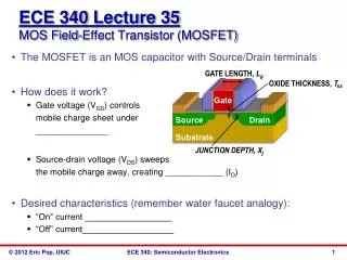
ECE 340 Lecture 33 MOS capacitor Threshold Voltage. Inversion: at V > V T (for NMOS), many electrons drawn to surface, which is now “inverted” vs. the p-doped substrate. Draw charge distribution: Draw energy bands at inversion:. Note:

E N D
ECE 340 Lecture 33MOS capacitor Threshold Voltage • Inversion: at V > VT (for NMOS), many electrons drawn to surface, which is now “inverted” vs. the p-doped substrate. Draw charge distribution: • Draw energy bands at inversion:
Note: • Mobile charge anywhere is given by difference between EC or EV and Fermi level as, e.g. n = NCexp(EC– EF) • If EF is close to EC then lots of __________________ • If EF is close to EV then lots of __________________ • At high gate V (> VT) which band is closer to EF? • The condition for this onset is ϕS = 2ϕF (see plot) qVi
At inversion (on p-type sub.) the mobile surface charges are ______________, such that numerically nsurf. = NA,sub. • Now we can calculate the threshold voltage, VT: • For NMOS (electron inversion on p-type substrate): • For PMOS (hole inversion on n-type substrate): • Net surface charge in inversion layer?
This is a good place to recap MOS capacitor behavior: • Since this is a capacitor, what does the C-V measurement look like?
ECE 340 Lecture 34MOS Capacitance-Voltage (C-V) curve • MOS capacitance measurement:
Why is there a difference in inversion capacitance at: • Low-frequency (<10 kHz) • High-frequency (~1 MHz) • Answer: Ci Ci Ci Ci
Inversion case I: inversion-layer (minority carriers!) can be supplied quickly to respond to changes in VG • How do we supply them? 1) Optical generation (turn lights on) 2) Providing a nearby source of minority carriers (like in a MOSFET) • Inversion case II: inversion-layer cannot be supplied quickly enough to respond to changes in VG Ci Ci Ci Ci Ci Ci
Ex: plot and label the C-V curve of a PMOS capacitor with P+ gate, substrate doping ND=5x1017 cm-3 and SiO2 d=2 nm
MOS capacitor non-idealities… in reality, neither the SiO2 nor the Si/SiO2 interface are perfect: • Mobile ions (Na+ used to be a major headache) • Dangling bonds at Si/SiO2 interface • Charge traps within SiO2 • We can group these non-idealities together as an equivalent sheet of charge Qi (>0) at the Si/SiO2 interface • + charge at the interface pulls down the E-bands there and changes the field across the SiO2 • This shifts the flat-band voltage:
Odd shifts in C-V characteristics were once a mystery: • Source of problem: Mobile ionic charge (e.g. Na+, K+) moving to/away from the interface, ΔVFB = Qi/Ci • Solution: cleaner environment, water, chemical supply. • With simple C-V measurements we can learn (and “debug”) a great deal about the properties and quality of MOS capacitors: • Obtain oxide thickness (d) from C accumulation • Obtain substrate doping (NA) from Cmin at VT (high-freq) • Interface charge (Qi) and VFB from C-V across various dox thicknesses
MOS capacitor wrap-up: • Experimental measurement of fast interface states (traps): Ci
A little more on the real measured C-V curve: • Effective oxide capacitance affected by: • Poly-silicon gate depletion (no problem with metal gate) • Finite thickness of inversion layer • Both of which are somewhat functions of voltage. • Last but not least: • Why HfO2 instead of SiO2? • Why metal gate instead of highly-doped poly-Si gate? Ci