Download
1 / 22
260 likes | 476 Views
FPGA Calculator Core. Project Characterization. Chen Zukerman Liran Moskovitch Advisor : Moshe Porian Duration : semesterial December 2011. Contents. Intro Project Overview Project Goals Requirements Architecture Micro Architecture Testability & GUI

E N D
FPGA Calculator Core Project Characterization Chen Zukerman LiranMoskovitch Advisor : Moshe Porian Duration: semesterial December 2011
Contents • Intro • Project Overview • Project Goals • Requirements • Architecture • Micro Architecture • Testability & GUI • Schedule
Intro • In many projects, there is a tradeoff between hardware and software implementation. • Hardware benefits: • Shorter computation time • Lower power consumption • Reduced physical size • Minimum resources • Good parallel processing capability • Software benefits: • Simple implementation • Reduced cost In this project we will focus on hardware implementation
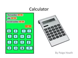
Project Overview • Hardware implementation of calculator core : • Positive integers • Operands: ‘+’ , ’-’ , ’x’ , ’/ ’ , ‘^’ , ‘ { ‘ , ‘ } ‘ • Order of operations • Manually acquisition Input via Matlab GUI • Result display - LCD + debugging feedback FPGA Feedback GUI Result
Project Goals • Hardware implementation using FPGA • Programming FPGA using VHDL • Implementation of Interactive GUI (MATLAB) • Experiencing full systemic perspective
Requirements • Hardware platform: Altera DE2 board - Cyclone II FPGA • Host communication via UART protocol • Internal communication via Wishbone protocol • Input - Data string to calculate • Output 1 - The calculated result displayed on the LCD • Output 2 – Confirmation of the result (software)
GUI 50 50 Yes x 5 ( 6 + 2 ^ 2 ) =
Data packet structure 8 bits SOP Type Header Address Client address + R/W Data Length Inner client address Data 0 . . . Data N-1 Packet CRC Tail EOP
UART Protocol start stop parity 8 bit word
RX PATH WBM1 Message decode to wishbone master Frame error Frame _ok type length address UART RX error Message Decoder UART_IN valid Data [7..0] RAM Data [7..0] CRC Read_enable Read_value
TXPATH WBS 2 Wishbone to Message encoder CRC Frame_finish WBM 3 UART TX crc UART_OUT Wishbone_data[7..0] Message encoder type address len valid Frame_OK busy Wishbone_data[7…0] RAM Write_enable
Calculator Core DATA wishbone WBS 1 wishbone WBM 2 Result to wishbone Result Reg Op Table
Calculator Algorithm ( ( ( 50 5 5 5 ( 5 x ( 6 + 4 ) ) 5 x ( 6 + 2 ^ 2 ) ( 5 x ( 6 + 2 ^ 2 ) ) 50 ( 5 x 10 ) x x x 10 10 ( ( ) 6 6 EOC + + 4 2 4 ) ^ ) ) EOC 2 ) EOC
Arithmetic Calculation Unit ^ Num1 (32 bit) DMUX x Res / Select op (3 bit) MUX + Num2 (32 bit) DMUX - Select op
LCD Core Result to LCD Binary to Ascii converter RAM (digits in Ascii code) WBS 3 Result from wishbone
LCD Register Select RS R/W’ E DB0 DB1 DB2 DB3 DB4 DB5 DB6 DB7 0: Write 1:Read Enable Result digits DATA
Clock & Reset Sys_clk = 100 [MHz] PLL Clk = 50[MHz] Reset_in Reset Block lock Sys_reset