Download
1 / 15
230 likes | 662 Views
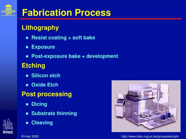
Lithography Resist coating + soft bake Exposure Post-exposure bake + development Etching Silicon etch Oxide Etch Post processing Dicing Substrate thinning Cleaving. Fabrication Process. Layer structure 205 Top Si layer 400nm Buried Oxide Wafer size 8” (200mm).

E N D
Lithography Resist coating + soft bake Exposure Post-exposure bake + development Etching Silicon etch Oxide Etch Post processing Dicing Substrate thinning Cleaving Fabrication Process
Layer structure 205 Top Si layer 400nm Buried Oxide Wafer size 8” (200mm) Step 1: Bare SOI wafer 205nm Si SiO2 400nm Si-substrate
Resist Shipley UV3 800nm thick Photoresist Step 2: Photoresist Coating
Step 3: Soft baking of resist Photoresist
AR coating No standing waves in resistduring lithography 40nm of NFC Step 4: Antireflective coating AR-coating
Step 5: Illumination • Deep UV Lithography • Wavelength = 248nm • NA = 0.63 • Dose = 10-40 mJ • Reduction = 4X
Etch properties TCP9400PTX ICP-RIE Low pressure /high density Cl2/HBr/He/O2 chemistry Two-step break-through main etch Step 8: Silicon etch
Etch properties Exelan Dual frequency Medium pressure /medium density CF4/CHF3 chemistry Step 9: Oxide Etch
Substrate thinning = dangerous Step 11: Protective Resist Layer • 1-3m resist cover 750m Wafer is diced into 3 x 3 cm2 dies for substrate thinning
Glue = Bee’s wax Heated to ± 130°C Bee’s wax Glass plate Step 12: Glue on glass plate
Mechanical grinding Alumina powder 5-8 hours Remove 500m 250m Bee’s wax Glass plate Step 13: Substrate thinning