Download
1 / 16
250 likes | 587 Views
Single-electron Devices. Speaker: Qiaoyan Yu qiaoyan@ece.rochester.edu ECE423 12-16-2006. Agenda. Milestone Motivations New characteristics Single-electron transistor (SET) Challenges Conclusions. Milestone. In 1909, Millikan first illustrated the manipulation of single electrons.

E N D
Single-electron Devices Speaker: Qiaoyan Yu qiaoyan@ece.rochester.edu ECE423 12-16-2006
Agenda • Milestone • Motivations • New characteristics • Single-electron transistor (SET) • Challenges • Conclusions
Milestone • In 1909, Millikan first illustrated the manipulation of single electrons. • In 1985, Dmitri Averin & Konstantin Likharev proposed single-electron transistor. • In 1987, Theodore Fulton & Gerald Doald at Bell lab fabricated and demonstrated SET.
Motivation • Power consumption challenges high performance and high density chip design • Faster and more information processing resulting in generating more heat flux • Reduce the corresponding charge per bit! Single-electron Device!!!
SED new characteristics • Exploit the quantum effect of tunneling • Control and measure the movement of single electron • Charge doest not flow continuously • Instead in a quantized way • Extremely high charge sensitivity • High precise for charge measurement
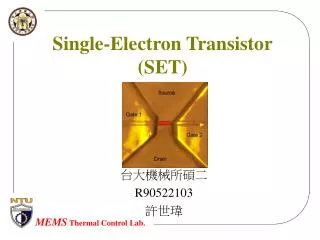
Single-electron transistor (SET) • Architecture • Equivalent circuit • Operation principle • I-V curve • SET VS. MOSFET
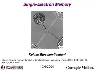
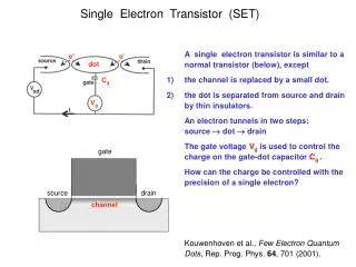
Tunnel junctions q island V2 V1 Source Drain +q1 -q1 +q2 -q2 C1 C2 gate Vb Cg Vg Architecture
SET vs. MOSFET • Structure • Two tunneling barrier vs. inversion channel • Size • Extremely small vs. large (although scaled down) • Main physical principle • Coulomb blockade vs. electron diffusion • Threshold voltage & source-drain current • Periodic vs. not periodic • Sensitivity • High vs. low (10000X) • Power • Low vs. high
SED challenges • Difficult to precisely control the device implementation • Characteristic of the device varies significantly from location to location • Suffer from “offset charges” • Randomly fluctuation of control signal
Conclusions • Because of natural small dimension, SED is a potential solution for continue silicon scaling. • It is not clear that SET replaces FET. • It is certain that quantum properties of electrons will be crucial in the design of electron devices. • Electron beam lithography and scanning probe techniques offer the best prospects for the future. • Some more esoteric techniques based on atomic particle deposition and colloid chemistry may also provide some benefits.
The End Thank You! Any questions?