Download
1 / 31
360 likes | 894 Views
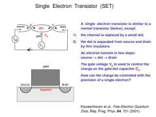
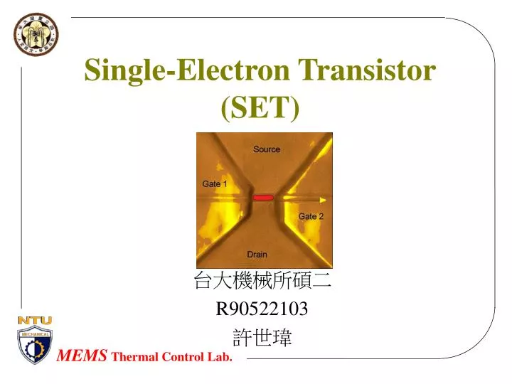
Single-Electron Transistor (SET). 台大機械所碩二 R90522103 許世瑋. What is SET?. Island 可為金屬或半導體材料 The charging energy should be larger than thermal energy--preventing the effect of thermal energy. E C =e 2 /2C Σ >k B T (determine operation temp)

E N D
Single-Electron Transistor(SET) 台大機械所碩二 R90522103 許世瑋
What is SET? • Island 可為金屬或半導體材料 • The charging energy should be larger than thermal energy--preventing the effect of thermal energy. EC=e2/2CΣ>kBT (determine operation temp) • The tunneling junction resistance should be larger than typical value Rj>h/ e2~25KΩ (Room temp. test)
Coulomb Blockade (CB) Transport in SET CB I-V curve
Single-electron MOS • 單電子半場效電晶體 (Minnesota Uni.)
Single-electron MOS • Self-aligned Floating Dot Gate—Fabrication Process Dry etching Wet etching (NH4OH:H2O2:H2O) Dry etching
Coulomb Blockade (CB) Transport in SET • 圖(a)之虛線,Q = CV,Q為總電荷數,在微小的 Quantum dot裡,電子電荷是量化的,是個不連續的量,加以不同的閘極電壓,連續的改變浮閘內的偏極電荷,所以浮閘內電荷雖仍是連續的量,但是因為庫倫阻斷效應,進入和離開浮閘內的電子並非同時進行,此時電子是一個接一個流動的,因此就可見到所謂的 Staircase of threshold voltage特性,如圖 (a)之實線。 • 圖(b)為 Conductance和閘極電壓之關係,由圖中可知 Conductance的振盪和流經浮閘的電荷數有極大的關係
Materials of High-Ea Island With Ea beyond ~100mev, exhibit noticeable Coulomb blockade oscillations at RT
Fabrication Method–V-PADOX • A Si wire with a fine trench across it on a SOI substrate. • Thermal oxidation is carried out just after the wire with a fine trench is defined.
Fabrication Process • Trench formation • Wire and side-gate definition • Top-gate definition
Comparison Twin Island
Twin Island • Wire width (a),(b)=60nm (c)=160nm • 由於熱應力的關係使得edge附近的oxidation rate減慢造成twin island • 形成island無需經過lithography definition的步驟
STM/AFM Nano-oxidation Process • 控制cantilever和Ti薄膜之間的電壓可以改變TiOx的厚度(width of island)
STM/AFM Nano-oxidation • Temperature Dependence(64nm) • Vb=6~10V(high bias) 電流主要是F-N tunneling,比較不受溫度的影響 • Vb=0.1~1V(low bias) 由於溫度產生thermion emission current造成電流有很大的變化(steep slope) High bias EF EF Low bias EF EF Width = 64nm
STM/AFM Nano-oxidation Temperature Dependence(10nm) • Weak temperature dependence Width = 10nm EF EF EF
Structure of SET(Ti) • Coulomb gap~50mV island
CNT-SET @ RT AU 電極 AFM施力方向 金屬型奈米碳管 Buckle 利用AFM使奈米碳管產生Buckle,造成電阻值變大~0.5M歐姆
@ 260K @ 30K 每個方塊的電子數目是固定的,可用Vg來控制電子進入island CNT-SET
Criteria For A good Single-electron Tunneling Memory • 操作溫度需在室溫(300K),或者至少能在液態氮的溫度(77K)並能有適當的bit error rate. • Low power consumption • 相同的讀、寫時間且循環時間短
Application • Nonvolatile Random-Access Memory (NOVORAM) • After capture, the electron changes the conductivity of the more conductive parts of this channel • The disadvantage of this geometry is that the grain geometry, and hence the memory cell switching thresholds, are inherently irreproducible
Application 在glass fiber上鍍上一Al薄膜,再exposure to oxygen形成一tunneling barrier(island) • Single-electron Transistor Scanning Electrometer(SETSE) 利用SET的特性,在tip與sample表面之間(~25nm)施加一電壓,藉由電流訊號來量測物件特性 2-Dimensional Electron Gas 做為金屬層
Application • Single-electron Transistor Scanning Electrometer(SETSE) Y-axial 隨著Vb的增加,SET的電流會有週期性的震盪(T~e/Cs) x-y plane
Application • Single-electron Transistor Scanning Electrometer(SETSE) • Cs:tip與sample電極間的電容,dependent on tip與2DEG的高度 • Total charge Q= • 表面電壓Vs:由電極和sample的work function差以及potential from charged centers distributed across and below the surface • Oscillation period T=e/Cs
e/Cs隨著tip接近表面而驟減 Bias Voltage~0.6V,減少SET和sample間的功函數差,如此可避免因tip產生的電場的干擾 Application • Single-electron Transistor Scanning Electrometer(SETSE)
Vs in xy plane with different height Height (A)95nm, (B)50nm, (C)25nm 隨著高度改變有不同的精度,不同diameter的tip決定最佳精度的高度 Application • Single-electron Transistor Scanning Electrometer(SETSE)
Photoactivity of single dopant atoms and surface traps in xy plane 利用光照射激發載子產生傳遞現象,亮點為新的正電荷,暗點為負電荷,sensitivity較好 Application • Single-electron Transistor Scanning Electrometer(SETSE)
Application • Single-electron Transistor Scanning Electrometer(SETSE) • 可探測到0.01e • 量測精度比EFM好而且無需施加較高的電壓(106Vcm-1) • 可描繪(image)並量測depletion regions, local capacitance, band bending, charge和表面的接觸電壓(contact potential)
Application • Radio-Frequency SET (RF-SET) • With Dual-Superconducting Quantum Interference Device (DSQUID) • Allow large operating speeds and extremely high charge sensitivity Tunneling junction
Application • 微型電腦 目前單電子電晶體的工作溫度已接近室溫,而且損耗小、電流-電壓曲線呈階梯形狀、功率低。單電子電晶體只需要一個電子就夠了,因此它的體積可以縮小到1%,所需電力減小到通常電晶體的10萬分之一。 • 超敏電流計 當外加一個磁場使單電子電晶體從超導態轉變為正常態時只要柵電極上有e/2電荷量的改變,每秒約109電子的電流就可以通過元件,它比通常的場效應電晶體對電荷的敏感度要強6倍。所以單電子電晶體可以利用這個性質製成高精度的電流計。
Reference • A. Nakajima, T. Futatsugi, K. Kosemura, T. Fukano, and N. Yokoyama, “Room temperature operation of Si single-electron memory with self-aligned floating dot gate,” Appl. Phys. Lett., vol. 70, pp. 1742–1744, Mar. 1997. • V. P. Roychowdhury and M. P. Anantram, “On computing with locally-interconnected architectures in atomic/nanoelectronic systems,” in Proc. IEEE Conf. Application-Specific Systems, Architectures, and Processors, 1997, pp. 14–23. • L. Guo, E. Leobandung, and Y. Chou, “A single-electron transistor memory operating at room temperature,” Science, vol. 275, pp. 649–651, Jan. 1997. • A. Nakajima, T. Futatsugi, K. Kosemura, T. Fukano, and N. Yokoyama, “Room temperature operation of Si single-electron memory with self-aligned floating dot gate,” Appl. Phys. Lett., vol. 70, pp. 1742–1744, Mar. 1997. • Henk W. Ch. Postma, Tijs Teepen, Zhen Yao,* Milena Grifoni, “Carbon Nanotube Single-Electron Transistors at Room Temperature,” 6 JULY 2001 VOL 293 SCIENCE • M. J. Yoo,* T. A. Fulton, H. F. Hess, R. L. Willett, L. N. Dunkleberger, R. J. Chichester, L. N. Pfeiffer, K. W. West, “Scanning Single-Electron Transistor Microscopy:Imaging Individual Charges,” SCIENCE z VOL. 276 z 25 APRIL 1997
Reference • C. Wasshuber etc., “Comparative Study of Single-Electron Memories,” IEEE, vol. 45, No.11, Nov. 1998. • Y. Takahashi, M. Nagase, H. Namatsu, K.Kurihara, K. Iwadate,Y. Nakajima, S. Horiguchi, K. Murase, and M. Tabe, “Conductance oscillations of a Si single-electron transistor at room temperature,” in IEDM Tech. Dig., 1994, pp. 938–940. • Y. Ono, Y. Takahashi, M. Nagase, H. Namatsu, K.Kurihara, K. Murase, “Fabrication Method for IC-Oriented Si Single-Electron Transistors,” IEEE., 2000. • K. Murase, M. Ishii, J. Shirakashi, K. Segawa, Y. Oka, “Comparision of experimental and theoretical results of room temperature operated Single-Electron Transistors made by STM/AFM nano-oxidation process,” IEEE., 2000. • KONSTANTIN K. LIKHAREV, “Single-electron devices and their applications,” PROCEEDINGS OF THE IEEE, VOL. 87, NO. 4, APRIL 1999 • R. J. Schoelkopf,* P. Wahlgren, A. A. Kozhevnikov, P. Delsing, D. E. Prober, “The Radio-Frequency Single-Electron Transistor (RF-SET): A Fast and Ultrasensitive Electrometer,” SCIENCE z VOL. 280 z 22 MAY 1998