Download
1 / 49
500 likes | 522 Views
CMOS Fabrication. EMT 251 Introduction to IC Design. Some Basics. Silicon Wafer. Silicon Lattice. Transistors are built on a silicon substrate Silicon is a Group IV material Forms crystal lattice with bonds to four neighbors. Dopants. Silicon is a semiconductor

E N D
CMOS Fabrication EMT 251 Introduction to IC Design
Silicon Lattice • Transistors are built on a silicon substrate • Silicon is a Group IV material • Forms crystal lattice with bonds to four neighbors
Dopants • Silicon is a semiconductor • Pure silicon has no free carriers and conducts poorly • Adding dopants increases the conductivity • Group V: extra electron (n-type) • Group III: missing electron, called hole (p-type)
p-n Junctions • A junction between p-type and n-type semiconductor forms a diode. • Current flows only in one direction
Power Supply Voltage • GND = 0 V • In 1980’s, VDD = 5V • VDD has decreased in modern processes • High VDD would damage modern tiny transistors • Lower VDD saves power • VDD = 3.3, 2.5, 1.8, 1.5, 1.2, 1.0, …
300mm Si wafer Integrated Circuit Technology “Planar” fabrication process: Simultaneous fabrication of many “chips” on a wafer, each comprising an integrated circuit (e.g. a microprocessor or memory chip) containing millions or billions of transistors Method: Sequentially lay down and pattern thin films of semiconductors, metals and insulators. • Materials used in a basic CMOS integrated circuit: • Si substrate – selectively doped in various regions • SiO2 insulator • Polycrystalline silicon – used for the gate electrodes • Metal contacts and wiring
Formation of Insulating Films • The favored insulator is pure silicon dioxide (SiO2). • A SiO2 film can be formed by one of two methods: • Oxidation of Si at high temperature in O2 or steam ambient • Deposition of a silicon dioxide film Applied Materials low-pressure chemical-vapor deposition (CVD) chamber ASM A412 batch oxidation furnace
Continuous gas flow Diffusion of reactants Boundary layer Deposited film Silicon substrate CVD Chemical Reactions • SiH4(gas) + O2(gas) SiO2(solid) + 2H2 (gas) • SiH4(gas) + H2(gas) +SiH2(gas) 2H2(gas) + PolySilicon (solid)
oxidation deposition ion implantation etching lithography Patterning the Layers Planar processing consists of a sequence of additive and subtractive steps with lateral patterning Lithography refers to the process of transferring a pattern to the surface of the wafer Equipment, materials, and processes needed: • A mask (for each layer to be patterned) with the desired pattern • A light-sensitive material (called photoresist) covering the wafer so as to receive the pattern • A light source and method of projecting the image of the mask onto the photoresist (“printer” or “projection stepper” or “projection scanner”) • A method of “developing” the photoresist, that is selectively removing it from the regions where it was exposed
We have exposed mask pattern, and developed the resist photoresist First: pattern photoresist Si oxide etchant … photoresist is resistant. SiO 2 Next: Etch oxide etch stops on silicon (“selective etchant”) Last: strip resist only resist is attacked Pattern Transfer by Etching In order to transfer the photoresist pattern to an underlying film, we need a “subtractive” process that removes the film, ideally with minimal change in the pattern and with minimal removal of the underlying material(s) • Selective etch processes (using plasma or aqueous chemistry) have been developed for most IC materials Jargon for this entire sequence of process steps: “pattern using XX mask”
The Photo-Lithographic Process optical mask Oxidation or thin-film deposition photoresist exposure photoresist photoresist coating removal (ashing) photoresist develop etch optional additional process step(s) spin, rinse, dry
Adding Dopants into Si Suppose we have a wafer of Si which is p-type and we want to change the surface to n-type. The way in which this is done is by ion implantation. Dopant ions are shot out of an “ion gun” called an ion implanter, into the surface of the wafer. Eaton HE3 High-Energy Implanter, showing the ion beam hitting the end-station Typical implant energies are in the range 1-200 keV. After the ion implantation, the wafers are heated to a high temperature (>1000oC). This “annealing” step heals the damage and causes the implanted dopant atoms to move into substitutional lattice sites.
Other than Ion Implantation.. • What else? • Diffusion
Interconnection Materials • Polysilicon interconnects are used to connect Gates and other short-distance connections which have minimal currents. Polysilicon is a very stable material that rarely interacts with nearby materials. • Metal interconnects have 3-5x the speed of polysilicon (electron mobility is higher) and less resistance. However, metals may react with nearby materials, and may have to be encapsulated using nitrides (e.g. Si3N4 or TiN) to prevent unwanted reactions, or partial erosion in subsequent etching procedures. This is expensive. In Upper Metallurgy (not local interconnects) metal is always used because processing is simple: only Metal + SiO2.
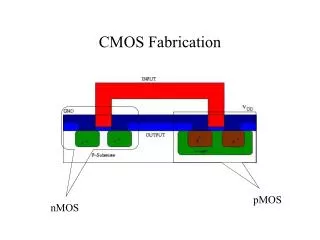
Schematic Cross-Sectional View Layout (Top View) N-channel MOSFET 4 lithography steps are required: 1. active area 2. gate electrode 3. contacts 4. metal interconnects channel width, W gate length, Lg
CMOS Technology Both n-channel and p-channel MOSFETs are fabricated on the same chip (VTp = -VTn ) • Primary advantage: • Lower average power dissipation • Ideally, in steady state either the NMOS or PMOS device is off, so there is no DC current path between VDD & GND • Disadvantages: • More complex (expensive) process • Latch-up problem (reduce by using highly doped substrate or wells)
transistor via Simple cross-section SiO2 metal3 metal2 metaal1 metaal1 poly substrate n+ n+ p+ substrate
Masks set • In MOSFET fabrication, mask set was used to define certain region on a silicon wafer. • The mask sets that used in standard fabrication are very expensive and not practical for education purposes.
CMOS Fabrication • CMOS transistors are fabricated on silicon wafer • Lithography process similar to printing press • On each step, different materials are deposited or etched • Easiest to understand by viewing both top and cross-section of wafer in a simplified manufacturing process
Inverter Cross-section • Typically use p-type substrate for nMOS transistor • Requires n-well for body of pMOS transistors • Several alternatives: SOI, twin-tub, etc.
Well and Substrate Taps • Substrate must be tied to GND and n-well to VDD • Metal to lightly-doped semiconductor forms poor connection called Shottky Diode • Use heavily doped well and substrate contacts / taps
Inverter Mask Set • Transistors and wires are defined by masks • Cross-section taken along dashed line
Detailed Mask Views • Six masks • n-well • Polysilicon • n+ diffusion • p+ diffusion • Contact • Metal
BasicSteps EMT 251 CMOS Fab
Fabrication Steps • Start with blank wafer • Build inverter from the bottom up • First step will be to form the n-well • Cover wafer with protective layer of SiO2 (oxide) • Remove layer where n-well should be built • Implant or diffuse n dopants into exposed wafer • Strip off SiO2
Oxidation • Grow SiO2 on top of Si wafer • 900 – 1200 C with H2O or O2 in oxidation furnace
Photoresist • Spin on photoresist • Photoresist is a light-sensitive organic polymer • Softens where exposed to light
Lithography • Expose photoresist through n-well mask • Strip off exposed photoresist 36
Etch • Etch oxide with hydrofluoric acid (HF) • Seeps through skin and eats bone; nasty stuff!!! • Only attacks oxide where resist has been exposed 37
Strip Photoresist • Strip off remaining photoresist • Use mixture of acids called piranah etch • Necessary so resist doesn’t melt in next step 38
n-well • n-well is formed with diffusion or ion implantation • Diffusion • Place wafer in furnace with arsenic gas • Heat until As atoms diffuse into exposed Si • Ion Implanatation • Blast wafer with beam of As ions • Ions blocked by SiO2, only enter exposed Si 39
Strip Oxide • Strip off the remaining oxide using HF • Back to bare wafer with n-well • Subsequent steps involve similar series of steps 40
Polysilicon • Deposit very thin layer of gate oxide • < 20 Å (6-7 atomic layers) • Chemical Vapor Deposition (CVD) of silicon layer • Place wafer in furnace with Silane gas (SiH4) • Forms many small crystals called polysilicon • Heavily doped to be good conductor
Polysilicon Patterning • Use same lithography process to pattern polysilicon
Self-Aligned Process • Use oxide and masking to expose where n+ dopants should be diffused or implanted • N-diffusion forms nMOS source, drain, and n-well contact
N-diffusion • Pattern oxide and form n+ regions • Self-aligned process where gate blocks diffusion • Polysilicon is better than metal for self-aligned gates because it doesn’t melt during later processing
N-diffusion • Historically dopants were diffused • Usually ion implantation today • But regions are still called diffusion
N-diffusion • Strip off oxide to complete patterning step
P-Diffusion • Similar set of steps form p+ diffusion regions for pMOS source and drain and substrate contact
Contacts • Now we need to wire together the devices • Cover chip with thick field oxide • Etch oxide where contact cuts are needed
Metallization • Sputter on aluminum over whole wafer • Pattern to remove excess metal, leaving wires