Download
1 / 27
290 likes | 415 Views
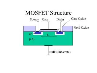
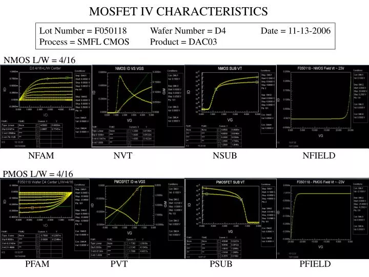
MOSFET IV CHARACTERISTICS. Lot Number = F050118 Wafer Number = D4 Date = 11-13-2006 Process = SMFL CMOS Product = DAC03. NMOS L/W = 4/16. NFAM NVT NSUB NFIELD. PMOS L/W = 4/16. PFAM PVT PSUB PFIELD. MOSFET EXTRACTED PARAMETERS.

E N D
MOSFET IV CHARACTERISTICS Lot Number = F050118 Wafer Number = D4 Date = 11-13-2006 Process = SMFL CMOS Product = DAC03 NMOS L/W = 4/16 NFAM NVT NSUB NFIELD PMOS L/W = 4/16 PFAM PVT PSUB PFIELD
MOSFET EXTRACTED PARAMETERS Lot Number = F050118 – Wafer Number = D4, Die Location R= , C=
MOSFET IV CHARACTERISTICS Lot Number = F050118 Wafer Number = D4 Date = 11-17-2006 Process = SMFL CMOS Product = DAC03 NMOS L/W = 2/16 NFAM NVT NSUB NFIELD PMOS L/W = 2/16 PFAM PVT PSUB PFIELD
MOSFET EXTRACTED PARAMETERS Lot Number = F050118 – Wafer Number = D4, Die Location R= , C=
Inverter Poly Van Der Pauw M1 Van Der Pauw N+ Van Der Pauw P+ Van Der Pauw P-Well Van Der Pauw M1 to Poly CBKR M1 to N+ CBKR M1 to P+ CBKR INVERTERS, VAN DER PAUW AND CBKR Lot Number = F050118 – Wafer Number = D4 , Die Location R= , C=
EXTRACTED PARAMETERS FROM INVERTERS, VAN DER PAUW AND CBKR Lot Number = F050118 – Wafer Number = D4 , Die Location R= , C=
73 Stage Ring at 5V, td = 0.712ns 73 Stage Ring at 6V, td = 0.228ns
Lot Number = F050118 Wafer Number = D1 Family of curves for L=2µm MOSFETs 2µm/32µm L/W NMOS AND PMOS
Lot Number = F050118 Wafer Number = D3 Family of curves for L=2µm MOSFETs 2µm/32µm L/W NMOS AND PMOS
Lot Number = F050118 Wafer Number = D3 Family of curves for L=4µm MOSFETs 2µm/32µm L/W NMOS AND PMOS
Lot Number = F050118 Wafer Number = D4 Family of curves for L=2µm MOSFETs 2µm/32µm L/W NMOS AND PMOS
nMOSFET VT WAFER MAP Lot Number = F050118 – Wafer Number = ??
MOSFET IV CHARACTERISTICS Lot Number = F050408 Wafer Number = D1 Date = 10-23-2006 Process = Sub-CMOS Product = Mixed NMOS L/W = 2/16 NFAM NVT NSUB NFIELD PMOS L/W = 2/16 PFAM PVT PSUB PFIELD
MOSFET EXTRACTED PARAMETERS Lot Number = F050408, Wafer Number = D1, Die Location R= , C=
Inverter Poly Van Der Pauw M1 Van Der Pauw N+ Van Der Pauw P+ Van Der Pauw P-Well Van Der Pauw M1 to Poly CBKR M1 to N+ CBKR M1 to P+ CBKR INVERTERS, VAN DER PAUW AND CBKR Lot Number = F050408, Wafer Number = D1, Die Location R= , C=
EXTRACTED PARAMETERS FROM INVERTERS, VAN DER PAUW AND CBKR Lot Number = F050408, Wafer Number = D1, Die Location R= , C=
Lot Number =F050408 Wafer Number =D3 Family of curves for L= 1µm MOSFETs 1 µm/ 16 µm L/W NMOS AND PMOS
Lot Number =F050408 Wafer Number =D1 Family of curves for L= 2µm MOSFETs 2 µm/ 16 µm L/W NMOS AND PMOS F050408 D1 Center 2/16
EXTRACTED PARAMETERS FROM Operational Amplifier Lot Number = F050408, Wafer Number = D1, Die Location R= , C=
EXTRACTED PARAMETERS FROM Ring Oscillator Lot Number = F050408, Wafer Number = D1, Die Location R= , C= gate delay td = 90ns/2/17= 2.6ns
nMOSFET VT WAFER MAP Lot Number = F , Wafer Number = D
MOSFET IV CHARACTERISTICS Lot Number = Wafer Number = Date = 11-13-2006 Process = Product = NMOS L/W = NFAM NVT NSUB NFIELD PMOS L/W = PFAM PVT PSUB PFIELD
MOSFET EXTRACTED PARAMETERS Lot Number = F , Wafer Number = D , Die Location R= , C=
Inverter Poly Van Der Pauw M1 Van Der Pauw N+ Van Der Pauw P+ Van Der Pauw P-Well Van Der Pauw M1 to Poly CBKR M1 to N+ CBKR M1 to P+ CBKR INVERTERS, VAN DER PAUW AND CBKR Lot Number = F , Wafer Number = D , Die Location R= , C=
EXTRACTED PARAMETERS FROM INVERTERS, VAN DER PAUW AND CBKR Lot Number = F , Wafer Number = D , Die Location R= , C=
Lot Number =F Wafer Number = Family of curves for L= µm MOSFETs µm/ µm L/W NMOS AND PMOS
nMOSFET VT WAFER MAP Lot Number = F , Wafer Number = D