Download
1 / 64
970 likes | 1.54k Views
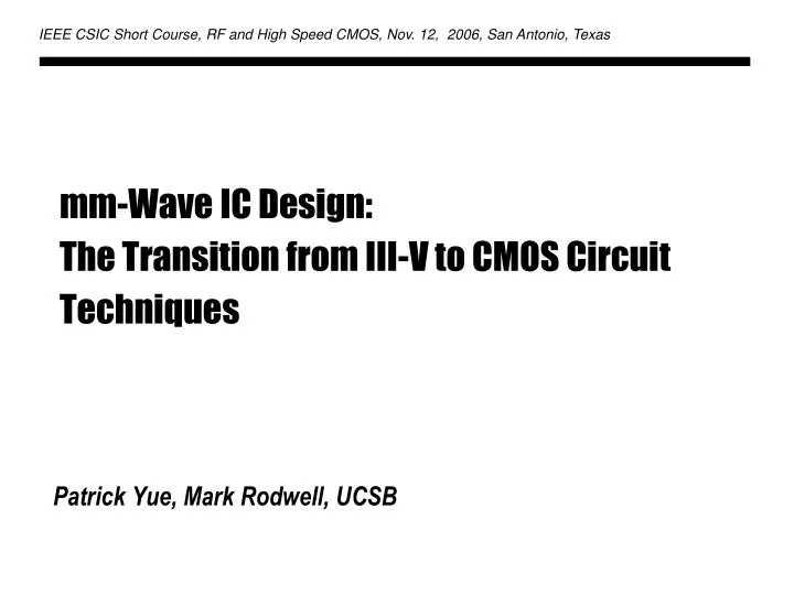
IEEE CSIC Short Course, RF and High Speed CMOS, Nov. 12, 2006, San Antonio, Texas. mm-Wave IC Design: The Transition from III-V to CMOS Circuit Techniques. Patrick Yue, Mark Rodwell, UCSB. Outline. Background Emerging mm-wave applications Open design issues for mm-Wave CMOS

E N D
IEEE CSIC Short Course, RF and High Speed CMOS, Nov. 12, 2006, San Antonio, Texas mm-Wave IC Design: The Transition from III-V to CMOS Circuit Techniques Patrick Yue, Mark Rodwell, UCSB
Outline • Background • Emerging mm-wave applications • Open design issues for mm-Wave CMOS • CMOS for mm-wave design • Optimizing CMOS device performance – layout & bias • On-chip inductors in CMOS • Cell-based device modeling and design methodology • State of the art CMOS mm-Wave design examples • mm-Wave design techniques • Device characterization issues • Unconditionally stable, gain-matched amplifier design procedure • Tuned amplifier, power amplifier design examples • On-chip transmission line design • Summary • References
Emerging mm-Wave Wireless Applications (~10 dB/km at sea level) • Unlicensed 60-GHz band for Gbit wireless link: • Outdoor, point-to-point wireless link • Wireless High-Definition Multimedia Interface (HDMI) • Licensed point-to-point wireless link in E-band (71-76, 81-86 GHz, and 92-95 GHz) • Vehicular radar at 76-77 GHz • 94-GHz band for high-resolution imaging Questions: Can we leverage scaled CMOS to produce more cost-effective products and enable new markets?
(S. Mehta, et al. ISSCC 2005.) 0.18-mm CMOS RF + baseband DSP Recent Evolution for CMOS RF RFFront-end Lower power, cost and size Baseband DSP (D. Su, et al. ISSCC 2002.) • 0.25-mm CMOS • 5-GHz RF transceiver But difficult to migrate below 0.18mm even for RF SoC...
State of the Art mm-Wave IC: 330 GHz 16-Finger Power Amp designs in progress: Michael Jones device: 5 V, 650 GHz fmax InP DHBT wiring: thin film microstrip with 2 um BCB Challenges: line losses are very high lines > 60 W are not feasible → increases Q of output tuning lines of required impedance are narrow → limits on DC current small unmodeled parasitics will de-tune design ....must maintain microstrip environment to device vias with negligible lengths of unmodeled random interconnects
Open Design Issues • RF CMOS design are by and large lumped circuits • mm-Wave design are traditionally distributed circuits • How will mm-Wave CMOS be designed? • Assuming that we will integrate an entire transceiver, should each block be impedance-matched? • Do we need new design flow / methodology? • Should all interconnect be modeled as T-line and be impedance-controlled? • Do we need a well-controlled global ground (plane)? • How to optimize CMOS device performance?
Strongly depend on layout Challenges for RF/mm-Wave in 0.13-mm CMOS and Beyond • High mask cost ($0.5M – $1M) • only makes sense if integration level increases, e.g. RF + large DSP, or mm-wave transceiver • Lack of a streamline RF/mm-wave design flow • Negative impact of technology scaling • Device • Process variations • Model uncertainty • Interconnect parasitic variations • Circuit • Low voltage headroom due to reduced Vdd • Develop a parasitic-aware design methodology • Explore low-voltage circuit techniques
High Frequency Figures of Merit • Minimize Rg, Rs, and Rsub for better performance • Layout and biasing are both critical • Minimize Rg, Rs, and Rsub for better performance • Layout and biasing are both critical
Rd Rsub1 Cgd_ext Rds Cds_ext Rg Cgd_ext Rsub2 Rs Complete Macro Model • Core model (baseline BSIM model) • Interconnect RC (3D EM field solver) • Gate and substrate resistances (physical model) Drain Core Model Bulk Gate Source
Gate Resistance Components Ref. 16
Gate Electrode Resistance Ref. 16 & 18
Channel Conductance (ac effect – channel charge distribution modulated by gate voltage, derived based on diffusion current) Ref. 16
Layout Guideline for Gate Resistance • Multi-finger layout in RF MOSFET is common to minimize Rgate(at the expense of more parasitic capacitance) • Typical finger width for 0.25um device is about 5 um whereas in 0.13um CMOS is 1.5 um • Total gate width ranges from a few 10’s of micron for LNA, mixer & VCO to a few millimeters for PA • Reltd (poly resistance) scales with 1/n2 • External portion of Rgeltd (contact resistance) scale with 1/n • Rch is independent of n to the first order
Substrate Resistance Model • Active and STI regions have different sheet resistances • Resistances in x and y directions modeled as parallel resistors Active Region STI Region (R. Chang, et al. TED 2004.)
Interconnect RC Modeling Using 3D Field Solver Source Gate • Wire capacitance per finger is extracted Drain Bottom view showing substrate taps Top view
RF Macro Model vs. Measurement (16 x 2m/0.12 m) Rg = 9.8 , Rsub = 475 , Cgs_ext= 4 fF, Cgd_ext= 2.9 fF, Cds_ext= 5.2 fF
Optimized Layout for fT, fmax and NF • Parallel Rg improves fmax and NFmin • Gate connected at both ends • Source drain metals do not overlap • Bulk contacts surround device
(E. Morifuji, et al. VLSI 1999.) fT (GHz) Finger width (mm) • Finger width â • No. of fingers á • Capacitance á • fT â Optimal Finger Width for fT (L.Tiemeijer, et al. IEDM 2004.) • fT approaches vsat / L deep in velocity saturation
(E. Morifuji, et al. VLSI 1999.) fmax (GHz) Finger width (mm) Optimal Finger Width for fmax (L.Tiemeijer, et al. IEDM 2004.) • Reducing Rg vs. increasing Cgg • For 0.13-mm, optimal finger width is ~2 mm • Optimal finger width decreases with device scaling fmax (GHz) Finger width (mm)
Finger width (um) Optimal Finger Width for NF Finger width (um) • Noise due to Rg and Rsub can be minimized through layout optimization Ref. 11
Optimal Biasing for fT, fMAX and NFMIN • Peak fT, fMAX and NFMIN characteristic current densities largely unchanged across technology nodes and foundries • NFMIN (0.15mA/µm) and peak fMAX (0.2mA/µm) are close LNAs simultaneously optimized for noise and high gain • In CMOS PAs optimum current swing when biased at 0.3mA/µm 10% degradation in fMAX Optimum Current Swing Bias Source: Yao, RFIC 2006. - U. of Toronto
First Patterned Ground Shield (PGS) • Inserted between the inductor and substrate • PGS fingers connected in a “star” shape • Terminates the E field • No effect on the H field • Improves isolation
4 layer (M5-M8) 3 layer (M6-M8) 2 layer (M7-M8) Self-Shielded Stacked Inductors for high SRF 25 mm • Self-shielded layout can effectively boost-strap the overlap capacitance * • 1-nH inductor can be achieved in 25x25 mm2 using M5 through M8 in a 0.13-mm CMOS 8-metal process * C.-C. Tang, JSSC, April 2002. Top view Bottom view
Design Automation Design Flexibility Systematic mm-wave Design with P-Cells • Stand-alone single device model is insufficient • Interconnect model accuracy limited by digital RC extraction • Test structure layout ¹actual circuit layout Model Scalability Model Accuracy Scalable Sub-Circuit P-Cells • Leverage the insight to device layout optimization • Exploit the modularity at the sub-circuit level
D1 D2 D D1&G2 G2 SS SS G1 D2&G1 S G1 G2 B Sample P-Cell Layouts and Circuit Models Cross-Coupled Pair Diff Pair Cascode
Inductor and transformer PCell Two transistor sub-circuit PCell Routing interconnect PCell Sub-Circuit Cell Library for mm-wave Design Tuned IF Amplifier • A unified design and modeling framework • Each sub-circuit P-Cell has its scalable circuit model
mm-wave P-Cell Characterization Test Structures • Measured S-parameters to validate macro models • UMC 0.13-mm CMOS with 8 copper layers
Outline • Background • Emerging mm-wave applications • Open design issues for mm-Wave CMOS • CMOS for mm-wave design • Optimizing CMOS device performance – layout & bias • On-chip inductors in CMOS • Cell-based device modeling and design methodology • State of the art CMOS mm-Wave design examples • mm-Wave design techniques • Device characterization issues • Unconditionally stable, gain-matched amplifier design procedure • Tuned amplifier, power amplifier design examples • On-chip transmission line design • Summary • References
140-220 & 220-330 GHz On-Wafer Network Analysis • HP8510C VNA, Oleson Microwave Lab mm-wave Extenders • coplanar wafer probes made by:GGB Industries, Cascade Microtech • connection via short length of waveguide • Internal bias Tee’s in probes for biasing active devices • measurements to 100 GHz can be in coax. GGB Wafer Probes330 GHz available with bias Tees
High Frequency Device Gain Measurements : Standard Pads Measuring wideband transistors is very hard ! Much harder than measuring amplifiers. Determining fmax in particular is extremely difficult on high-fmax or small devices Standard "short pads"must strip pad capacitancemust strip pad inductance--or ft will be too high !cal can be bad due to substrate coupling make pads small, and shield them from substratecal can be bad due to probe coupling use small probe pitch, use well-shielded probes
High Frequency Measurements : On-Wafer LRL Extended Reference planestransistors placed at center of long on-wafer lineLRL standards placed on waferlarge probe separation → probe coupling reducedstill should use the best-shielded probes available Problem: substrate mode couplingmethod will FAIL if lines couple to substrate modes→ method works very poorly with CPW linesneed on wafer thin-film microstrip lines CPW
Design Tools: Power Gain Definitions Transducer Gain Available Gain Insertion Gain Operating Gain Maximum Available Gain After impedance-matching: ....but only if unconditionally stable...
Design Tools: Stability Factors, Stability Circles Load Stability Circle Source Stability Circle Negative port impedance→ negative-R oscillator Tuning for highest gain→ infinite gain (oscillation)
Design Tools: Maximum Stable Gain circles at 50 GHz 17 W circle stabilization methods MSG results MAG 50 GHz Adding series/shunt resistance excludes source or load from unstable regions → stabilizes
Design Procedure: Simple Gain-Matched Amplifier First: stabilize at the design frequency ---device is potentially unstable at 100 GHz design frequency source stability circle: ~5 Ohm on input willoverstabilize the device After stabilizing(slightly over-stabilizing)
Design Procedure: Simple Gain-Matched Amplifier available gain operating gain Second: Determine required interface impedances The Ga & Gp circles define the source & load impedances which the transistor must see ...it is necessary to OVERSTABILIZE the device to move the Ga & Gp circles towards the Smith chart center Third: Design Input & Output Tuning Networks ...to provide these impedances... ...added to device, the amplifier is not yet complete...
Design Procedure: Simple Gain-Matched Amplifier source & load stability circles & 10,20,...,100 GHz Forth: Add out-of-band stabilization potentially unstable below 75 GHz with frequency-selective series stabilization ...caused only slight mistuning & slight gain drop @ 100 GHz ...and is unconditionally stable above 10 GHz
Design Procedure: Effect of Line Losses Finally: adjusting for line losses high line skin effect losses → reduced gain but line losses also increase stability factor loss in gain are partly recoveredby reducing stabilization resistance &re-tuning the design --no analytical procedure; just component tweaking line losses line losses have severe impact ...in VLSI wiring environment ...particularly at 50 + GHz ...particularly with high-power amplifiers
Tuned Amplifier Examples 3-stage cascode in 180 nm CMOS III-V HBT small-signal amplifiers Note: simple gain-tuned amplifiers → limited applicationsTransmitters need power amplifiers: need output loadline-match, not gain-matchReceivers need low-noise amplifiers: need input noise-match, not gain-match
Power Amplifier Design (Cripps method) For maximum saturated output power, & maximum efficiency device intrinsic output must see optimum loadline set by: breakdown, maximum current, maximum power density. parasitic C's and R's represented by external elements... ammeter monitors intrinsic junction currentwithout includingcapacitive currents ...(Vcollector-Vemitter ) measures voltageinternal to series parasitic resistances...
Power Amplifier Design (Cripps Method) Design steps are 1) input stabilization (in-band) 2) output tuning for correct load-line 3) input tuning (match) 4) out-of-band stabilization Example: 60 GHz, 30 mW PA, 130 nm BiCMOS
Design: Multi-Finger Power Amplifiers: Even-mode method Even-mode equivalent circuit -- Most multi-finger amplifiers do not use Wilkinson combiners: lines are too longEven-mode equivalent circuit maps combined design into single-device design Final design tuning (E&M simulation) with full circuit model This method explicitly models all feed parasitics in a large multi-finger transistorMUCH more reliable than using single lumped model for multi-finger device
Design: Multi-Finger Amplifiers: spatial mode instabilities If each transistor finger is individually stabilized, high-order modes are stable. Amplifier layout usually does not allow sufficient space for this. All spatial modes must then be stabilized. Stabilization method: bridging resistors → parallel loading to higher-order modesSelect so that (ZS , ZL) presented to device lie in the stable regions etc...
Design: Multi-Finger Amplifiers: Layout Examples W-band InP HBT power amplifier - UCSB mm-wave InP HBT power amplifier - Rockwell mm-wave InP HBT power amplifier - Rockwell