Download
1 / 18
230 likes | 581 Views
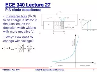
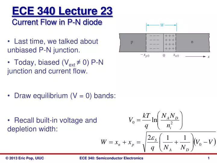
ECE 340 Lecture 23 Current Flow in P-N diode. Last time, we talked about unbiased P-N junction. Today, biased ( V ext ≠ 0) P-N junction and current flow. Draw equilibrium (V = 0) bands: Recall built-in voltage and depletion width:. Qualitative band diagrams with applied voltage:

E N D
ECE 340 Lecture 23Current Flow in P-N diode • Last time, we talked about unbiased P-N junction. • Today, biased (Vext≠ 0) P-N junction and current flow. • Draw equilibrium (V = 0) bands: • Recall built-in voltage and depletion width:
Qualitative band diagrams with applied voltage: • Current flow in equilibrium (V = 0):
Qualitatively expect I-V curve to be: • In forward bias, inside space charge region (SCR): • Where V is the applied bias and ___________________
Let’s look at the injected minority carriers: • On the n-side, injected holes. • Just at the edge of n-side depletion region:
Excess injected holes diffuse into the n-side: (same is true of excess injected electrons on p-side). • Injected hole diffusion current: • Where equilibrium hole concentration pn0 = (and similar for injected electron diffusion on p-side, just replace subscripts p with n) • Hole diffusion current proportional to excess hole concentration at any distance x into the n-type region. • Due to hole current continuity, we can evaluate at x=xn0=0
We can also write diffusion current for electrons in p-side: • Now total current
ECE 340 Lectures 24-26P-N diode carrier injection; reverse bias & breakdown Recap diode bias diagrams: • equilibrium • forward bias (V > 0) • reverse bias (V < 0)
Recap some of the equations: • Depletion width (decreases at forward bias, increases at reverse bias) • Maximum electric field (decreases at forward bias, increases at reverse bias) • Built-in voltage • Charge stored
Current density (current I = J∙A) • What about an asymmetrically doped junction? Say, p side much more heavily doped (NA >> ND): • Remember, current is due to minority carrier injection • Typically p-n junctions in real life are made by counterdoping. E.g. start with p-type wafer and dope with ND only at the surface to obtain junction. Eqs. so far readily apply if • NA = net doping on p-side = (NA – ND)p-side • ND = net doping on n-side = (ND – NA)n-side
Ex: a p-n junction has NA=1019 cm-3 and ND=1016 cm-3. The applied voltage is 0.6 V. a) What are the minority carrier concentrations at the edges of the depletion region? b) What are the excess minority carrier concentrations? c) Sketch δn(x) on the p-side if recombination lifetime is 2 μs.
Current continuity along junction length, JTOT = const. • As carriers recombine (deep into n- or p-side) the diffusion current is replaced by _____________ • But, we were able to deduce current equation by simple diffusion arguments at the _________________ where the E-field was just barely zero.
Reverse bias: • Depletion region widens • E-field across depletion region _________________ • Current is due only to minority carrier ______________ across the junction • Current is supplied by EHP generation in the __________________ (what if I change the temperature or turn on the light?) • Recall, J0 =
Junction breakdown when E-field exceeds a critical value. If current continues increasing, then diode ______________ .
P-N junction breakdown (3 types) 1) Zener breakdown: • Dominant for heavily doped (>1018 cm-3) p+n+ diodes • Breakdown at a few Volts (typically < 5 V) • Electron tunneling from filled valence states on p-side into (mostly) empty conduction band states on n-side
2) Avalanche breakdown • More lightly doped junctions (<1017 cm-3) • Wider depletion region, electrons accelerated across it gain enough energy to create additional EHPs • Impact ionization and carrier multiplication
Empirical observation of VBR with doping and material • VBR decreases with increasing N (=NA or ND) • VBR decreases with decreasing EG • Breakdown dependence on temperature: • For tunneling (Zener) breakdown… • For avalanche breakdown…
3) Punchthrough breakdown: • Occurs when either depletion region “punches through” the entire length of the diode, e.g. xn(V) = Ln Ln