Download
1 / 2
20 likes | 302 Views
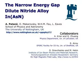
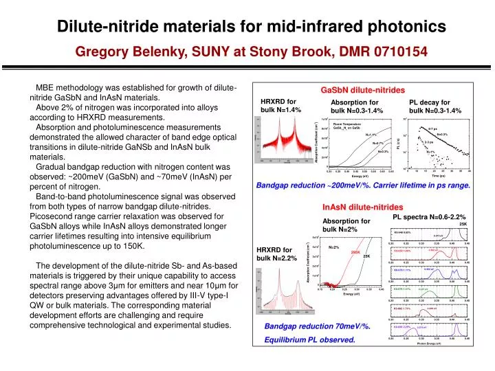
Dilute-nitride materials for mid-infrared photonics Gregory Belenky, SUNY at Stony Brook, DMR 0710154. MBE methodology was established for growth of dilute-nitride GaSbN and InAsN materials. Above 2% of nitrogen was incorporated into alloys according to HRXRD measurements.

E N D
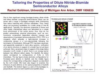
Dilute-nitride materials for mid-infrared photonicsGregory Belenky, SUNY at Stony Brook, DMR 0710154 MBE methodology was established for growth of dilute-nitride GaSbN and InAsN materials. Above 2% of nitrogen was incorporated into alloys according to HRXRD measurements. Absorption and photoluminescence measurements demonstrated the allowed character of band edge optical transitions in dilute-nitride GaNSb and InAsN bulk materials. Gradual bandgap reduction with nitrogen content was observed: ~200meV (GaSbN) and ~70meV (InAsN) per percent of nitrogen. Band-to-band photoluminescence signal was observed from both types of narrow bandgap dilute-nitrides. Picosecond range carrier relaxation was observed for GaSbN alloys while InAsN alloys demonstrated longer carrier lifetimes resulting into intensive equilibrium photoluminescence up to 150K. The development of the dilute-nitride Sb- and As-based materials is triggered by their unique capability to access spectral range above 3μm for emitters and near 10μm for detectors preserving advantages offered by III-V type-I QW or bulk materials. The corresponding material development efforts are challenging and require comprehensive technological and experimental studies. GaSbN dilute-nitrides HRXRD forbulk N=1.4% Absorption forbulk N=0.3-1.4% PL decay forbulk N=0.3-1.4% Bandgap reduction ~200meV/%. Carrier lifetime in ps range. InAsN dilute-nitrides PL spectra N=0.6-2.2% Absorption forbulk N=2% HRXRD forbulk N=2.2% Bandgap reduction 70meV/%. Equilibrium PL observed.
Dilute-nitride materials for mid-infrared photonicsGregory Belenky, SUNY at Stony Brook, DMR 0710154 The overall project is focused at development of materials with controlled parameters for infrared optoelectronics. This part of the project is aimed at development and use of a new type of heterostructures for fabrication of semiconductor lasers. The interdisciplinary nature of the project provides excellent training for graduate students. The project includes collaborative efforts of Stony Brook University, Department of Electrical and Computer Engineering (ECE) and St. Petersburg State Polytechnic University, Russia. The work includes participation of 9 graduate (Ph. D.) students. Research group of St.Petersburg State Polytechnic University, Russia, headed by Prof. Leonid Vorobyev (second from left). (From left) Zerova Vera, Melentjev Grigori (grad.st.), Thumrongsilapa Paphavee (grad.st.), Shalygin Vadim, Sofronov Anton (grad.st.), Chernyshova Ekaterina (grad.st.), Panevin Vadim (grad.st.) Optoelectronics Group of the Department of ECE, SUNY at Stony Brook. Top row: (From Left): Faculty- Sergey Suchalkin, Gela Kipshidze, Dmitri Donetski, post doctoral fellow- Yong Qiang Wang. Bottom row: graduate students: Takashi Hosoda, Seungyong Jung, Jianfeng Chen, Ding Wang.