Download
1 / 76
780 likes | 798 Views
A Lecture On Operational Amplifier (OP-AMP). by. S K Rai Electronics Engineering Department BKBIET, CEERI Road Pilani (Raj.)-333 031. General Amplifier. 2. Operational Amplifier: OP - AMP is a solid state device capable of sensing and amplifying dc and ac input signals.

E N D
A LectureOnOperational Amplifier(OP-AMP) by S K Rai Electronics Engineering Department BKBIET, CEERI Road Pilani (Raj.)-333 031
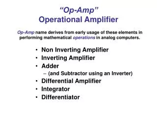
Operational Amplifier: OP - AMP is a solid state device capable of sensing and amplifying dc and ac input signals. The word “operational” is used because the amplifier can be used to perform a variety of mathematical operations such as addition, subtraction, integration, differentiation etc. The operational amplifier is a direct-coupled high gain amplifier usable from 0 to over 1MH Z to which feedback is added to control its overall response characteristic i.e. gain and bandwidth. The op-amp exhibits the gain down to zero frequency. Such direct coupled (dc) amplifiers do not use blocking (coupling and by pass) capacitors since these would reduce the amplification to zero at zero frequency. Large by pass capacitors may be used but it is not possible to fabricate large capacitors on a IC chip. The capacitors fabricated are usually less than 20 pf. Transistor, diodes and resistors are also fabricated on the same chip. Differential amplifier is a basic building block of an op-amp. 3
Types of Differential Amplifier: • The four differential amplifier configurations are following: • Dual input, balanced output differential amplifier • OR Differential input, differential output differential amplifier • OR double ended input, double ended output differential amplifier • Dual input, unbalanced output differential amplifier. • OR Differential input, single ended output differential amplifier • OR Double ended input, single ended output differential amplifier • Single input, balanced output differential amplifier. • Single input, unbalanced output differential amplifier. 4
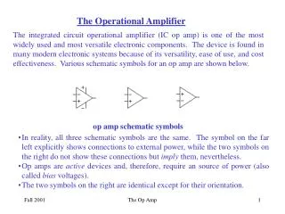
Symbol of Operational Amplifier: + V+ ↔ +VCC V- ↔ -VEE or -Vcc The Gain of OP-AMP is denoted by “A”. A = (Output/Difference Between Two Input Signals) = Vo /( V1 – V2 ) Where, V1 = Voltage Applied at Non-Inverting input V2 = Voltage Applied at Inverting input Vo = Output Voltage V+ inverting input output non-inverting input V 5
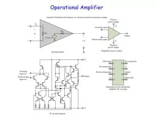
Block Diagram of OP-AMP: Input stage: It consists of a dual input, balanced output differential amplifier. Its function is to amplify the difference between the two input signals. It provides high differential gain, high input impedance and low output impedance. Intermediate stage: The overall gain requirement of an Op-Amp is very high. Since the input stage alone cannot provide such a high gain. Intermediate stage is used to provide the required additional voltage gain. It consists of another differential amplifier with dual input, and unbalanced ( single ended) output. 6
Block Diagram of OP-AMP: Buffer and Level shifting stage:As the Op-Amp amplifies D.C signals also, the small D.C. quiescent voltage level of previous stages may get amplified and get applied as the input to the next stage causing distortion the final output. Hence the level shifting stage is used to bring down the D.C. level to ground potential, when no signal is applied at the input terminals. Buffer is usually an emitter follower used for impedance matching. Output stage:It consists of a push-pull complementary amplifier which provides large A.C. output voltage swing and high current sourcing and sinking along with low output impedance. 7
OP-AMP ICs: (+) Notch µA741 (-) DIP-741 Dual op-amp 1458 device DIP: Dual inline package 4 3 2 1 8
DIFFERENTIAL AND COMMONMODE OPERATION : Differential Inputs: When separate inputs are applied to the op-amp, the resulting difference signal is the difference between the two inputs. Common Inputs: When both input signals are the same, a common signal element due to the two inputs can be defined as the average of the sum of the two signals. Output Voltage: Since any signals applied to an op-amp in general have both in-phase and out-phase components, the resulting output can be expressed as- Where, Vd: difference voltage Vc: common voltage Ad: differential gain of the amplifier Ac: common-mode gain of the amplifier 10
OP-AMP Parameters: Input offset Voltage : Input offset voltage is the voltage that must be applied between the two input terminals of an op-amp to null the output. Vio = Vdc1 – Vdc2 Input offset Current: The algebraic difference between the current in the inverting and non inverting terminal is known as the input offset current Iio = (IB1 – IB2). Input Bias Current: IB is the average current flows in the inverting and non-inverting terminal of an op-amp. IB = (IB1 + IB2 )/2 Open Loop Voltage gain: It is the ratio of the output voltage and the differential input voltage A = Output voltage/Differential input = Vo/Vid 11
OP-AMP Parameters: Output offset Voltage : Output offset voltage is the output voltage when both the input terminals are grounded. Output Voltage Swing: This parameter indicates the values of positive and negative saturation voltage of the op-amp. Differential input resistance(Ri): Differential input resistance Ri is the equivalent resistance that can be measured at either the inverting or non-inverting input terminals with the other terminal connected to ground. Input Capacitance (Ci): Input capacitance is the equivalent capacitance that can be measured at either the inverting or non-inverting input terminal with the other terminal connected to ground. Common Mode Rejection Ratio(CMRR): When the same voltage is applied to both the input terminals the voltage is called a common mode voltage Vcm and the op-amp is said to be operating in the common mode configuration,CMRR is defined as the ratio of the differential voltage gain to common mode gain. CMRR = Ad/Acm Supply voltage Rejection Ratio: The change in an op-amps input offset voltage Vio caused by variations in the supply voltage is called the SVRR. It is expressed in microvolts per volt or in decibels. SR= ΔVio/ΔV (µV/V or dB) 12
OP-AMP Parameters: Slew Rate: Slew rate is defined as the maximum rate of change of output voltage per unit of time and is expressed as volt per micro second. SR=(I dVo/dt I)max(V/μs) v desired output waveform v t t actual output because of slew rate limitation 13
OP-AMP Parameters: Gain Bandwidth Product : The gain bandwidth product(GB) is the bandwidth of the op-amp when the voltage gain is 1. Ideal Vs Practical Parameters of OP-AMP : 14 Note: Please Remember all these values for µA741.
Q. Determine the output voltage of an op-amp for input voltages of Vi1 150 V, Vi2 140 V. The amplifier has a differential gain of Ad=4000 and the value of CMRR is: (a) 100. (b) 105. Ans: (a) (b) 15
Frequency-Gain Relation: • Ideally, signals are amplified from DC to the highest AC frequency • Practically, bandwidth is limited • 741 family op-amp have an limit bandwidth of few KHz. • Unity Gain frequency f1: the gain at unity • Cutoff frequency fc: the gain drop by 3dB from dc gain Gd. 20log(0.707)=-3dB GB Product : f1 = Gdfc 16
Q. Determine the cutoff frequency of an op-amp having a unit gain frequency f1 = 10 MHz and voltage differential gain Gd = 20V/mV. ? Hz 10MHz • Sol: • Since f1 = 10 MHz • By using GB production equation • f1 = Gd fc • fc = f1 / Gd = (10 MHz) / (20 V/mV) • = (10 X 106) / (20 X 103) • = 500 Hz 17
Concept of Virtual ground: We know that, an ideal Op-Amp has perfect balance (ie output will be zero when input voltages are equal). Hence when output voltage Vo = 0, we can say that both the input voltages are equal ie V1 = V2. Since the input impedances of an ideal Op-Amp is infinite ( Ri = inf). There is no current flow between the two terminals. Hence when one terminal ( say V2 ) is connected to ground (ie V2 = 0) as shown. Then because of virtual ground V1 will also be zero. +VCC V1 =V2 =0 Vo V2 =0 -VEE 18
Open Loop OP-AMP Configuration : • There are three Open loop Configuration Namely: • Differential OP-AMP • Inverting OP-AMP • Non-inverting OP-AMP Inverting OP-AMP v1= 0, v2 = vin. vo = -Ad vin Differential OP-AMP v1 = vin1 and v2 = vin2. vo = Ad (vin1 – vin2 ) Non-Inverting OP-AMP v1 = +vin , v2 = 0 vo = +Ad vin 19
OP-AMP with Feedback : • Since OP-AMP gain A is very large, thus when operated in open loop, the OP-AMP goes into saturation. • The gain of amplifier can be controlled by modifying the basic circuit i.e. adding feedback. Generally the negative feedback is added, which reduces the gain and also added other advantages. • A closed loop amplifier can be represented by two blocks one for an OP-AMP and other for a feedback circuits. There are four following ways to connect these blocks. The Basic configuration of feedback is given below: • Voltage – series feedback • Voltage – shunt feedback • Current – series feedback • Current – shunt feedback 20
Op-Amp “Golden Rules” • When an op-amp is configured in any negative-feedback arrangement, it will obey the following two rules: • The inputs to the op-amp draw or source no current (true whether negative feedback or not) • The op-amp output will do whatever it can (within its limitations) to make the voltage difference between the two inputs zero. 21
Voltage series feedback: It is also called non-inverting voltage feedback circuit. With this type of feedback, the input signal drives the non-inverting input of an amplifier; a fraction of the output voltage is then fed back to the inverting input. The op-amp is represented by its symbol including its large signal voltage gain Ad or A, and the feedback circuit is composed of two resistors R1 and Rf. 22
Voltage shunt Feedback: It is also called inverting voltage feedback circuit. Input Impedance: Output Impedance: iO = ia + ib Since RO is very small as compared to Rf +(R1 || R2 ) Therefore,i.e. iO= ia vO = RO iO + A vd. vd= vi – v2 = 0 - B vO 23
OP-AMP Applications Analog Inverter and Scale Changer: Assuming OPAMP to be an ideal one, the differential input voltage is zero. i.e. vd = 0 Therefore, v1 = v2 = 0 Since input impedance is very high, therefore, input current is zero. OPAMP do not sink any current. iin= if vin / R = - vO / Rf vo = - (Rf / R) vin If R = Rf then vO = -vin, the circuit behaves like an inverter. If Rf / R = K (a constant) then the circuit is called inverting amplifier or scale changer voltages. 24
OP-AMP Applications Inverting summer: for an ideal OPAMP, v1 = v2. The current drawn by OPAMP is zero. Thus, applying KCL at v2 node. This means that the output voltage is equal to the negative sum of all the inputs times the gain of the circuit Rf/ R; hence the circuit is called a summing amplifier. When Rf= R then the output voltage is equal to the negative sum of all inputs. vo= -(va+ vb+ vc) 25
OP-AMP Applications Inverting summer: If each input voltage is amplified by a different factor in other words weighted differently at the output, the circuit is called then scaling amplifier. The circuit can be used as an averaging circuit, in which the output voltage is equal to the average of all the input voltages. In this case, Ra= Rb= Rc = R and Rf / R = 1 / n where n is the number of inputs. Here Rf / R = 1 / 3. vo = -(va+ vb + vc) / 3 In all these applications input could be either ac or dc. 26
OP-AMP Applications Non-inverting summer: If the input voltages are connected to non-inverting input through resistors, then the circuit can be used as a summing or averaging amplifier through proper selection of R1, R2, R3 and Rf. as shown. To find the output voltage expression, v1 is required. Applying superposition theorem, the voltage v1 at the non-inverting terminal is given by Hence the output voltage is: 27
OP-AMP Applications Non-inverting summer: This shows that the output is equal to the average of all input voltages times the gain of the circuit (1+ Rf / R1), hence the name averaging amplifier. If (1+Rf/ R1) is made equal to 3 then the output voltage becomes sum of all three input voltages. vo = v a + vb+ vc Hence, the circuit is called summing amplifier. 28
Q. Find the gain of VO / Vi of the circuit. Sol: Current entering at the inveting terminal Applying KCL to node 1, Applying KCL to node 2, Thus the gain A = -8 V / VO 29
Q. Find a relationship between VO and V1 through V6 in the circuit . 30
Sol: VO = V2 + V4 + V6 - V1 - V3 - V5. 31
Q. (a) Show that the circuit of given figure has A = VO / Vi = - K (R2 / R1) with K = 1 + R4 / R2 + R4 / R3, and Ri = R1. (b) Specify resistance not larger than 100 K to achieve A = -200 V / V and Ri = 100 K. 32
Sol: 33
OP-AMP Applications Integrator: The output voltage is directly proportional to the negative integral of the input voltage and inversely proportional to the time constant RC. If the input is a square wave, the output will be a triangular wave. For accurate integration, the time period of the input signal T must be longer than or equal to RC. 34
Q. Prove that the network shown in figure is a non-inverting integrator with The voltage at point A is vO / 2 and it is also the voltage at point B because different input voltage is negligible. vB = VO / 2 Therefore, applying Node current equation at point B, 35
OP-AMP Applications Differentiator: Thus the output vo is equal to the RC times the negative instantaneous rate of change of the input voltage vin with time. A sine wave input produces cosine output. The input signal will be differentiated properly if the time period T of the input signal is larger than or equal to Rf C. T ≥Rf C As the frequency changes, the gain changes. Also at higher frequencies the circuit is highly susceptible at high frequency noise and noise gets amplified. Both the high frequency noise and problem can be corrected by adding, few components. 36
OP-AMP Applications Differential Amplifier: - Since there are two inputs superposition theorem can be used to find the output voltage. When Vb= 0, then the circuit becomes inverting amplifier, hence the output due to Va only is Vo(a) = -(Rf / R1) Va Similarly when, Va = 0, the configuration is a inverting amplifier having a voltage divided network at the non-inverting input 37
Q. Find vout and iout for the circuit shown in figure. The input voltage is sinusoidal with amplitude of 0.5 V. We begin by writing the KCL equations at both the + and – terminals of the op-amp. For the negative terminal, Therefore, 15 v- = vout For the positive terminal, This yields two equations in three unknowns, vout, v+ and v-. The third equation is the relationship between v+ and v- for the ideal OPAMP, v+ = v- Solving these equations, we find vout = 10 vin = 5 sinωt V Since 2 kΩ resistor forms the load of the op-amp, then the current iout is given by 38
Q. For the different amplifier shown in figure, verify that An instrumentation amplifier is a differential op-amp circuit providing high input impedances with ease of gain adjustment through the variation of a single resistor (R3 in the Figure if other resistances are equal). Since the differential input voltage of OPAMP is negligible, therefore, v1= vxand v2 = vy The input impedance of OPAMP is very large and, therefore, the input current of OPAMP is negligible. Amd The OPAMP3 is working as differential amplifier, therefore, 39
Q. Obtain an expression of the type iO = Vi / R - VO / RO for the circuit shown in fig. Hence verify that if R4 / R3 = R2 / R1 the circuit is a V-I converter with RO =∞ and R = R1 R5 / R2. iO = current through the resistor. 40
Q. Design an amplifier with a gain of +9 and Rf =12 KΩ using an op-Amp. Soln: Since the gain is positive: Choose a non-inverting amplifier Then we have, Gain is, 41
Q. A 5 mV peak voltage, 1 KHz signal is applied to the input of an Op-Amp integrator for which R=100KΩ and C=1μF. Find the output voltage. Soln: Given R=100KΩ C=1μF Vm =5mV F=1KHz V0 =? We have Vi = Vm Sinwt = VmSin2пft Vi=5sin2000пt mV For an integrator, 42
Q. The input to a differentiator is a sinusoidal voltage of peak value 5mV and frequency 2KHz . Find the output if R = 100KΩ and C=1μF. Soln: 43
OP-AMP Applications : - Since there are two inputs superposition theorem can be used to find the output voltage. When Vb= 0, then the circuit becomes inverting amplifier, hence the output due to Va only is Vo(a) = -(Rf / R1) Va Similarly when, Va = 0, the configuration is a inverting amplifier having a voltage divided network at the non-inverting input 40
- 555 40
What is a 555 Timer? • The 555 timer is an 8-pin IC that is capable of producing accurate time delays and/or oscillators. • In the time delay mode, the delay is controlled by one external resistor and capacitor. • In the oscillator mode, the frequency of oscillation and duty cycle are both controlled with two external resistors and one capacitor.
Capacitor • A capacitor is an electrical component that can temporarily store a charge (voltage). • The rate that the capacitor charges/discharges is a function of the capacitor’s value and its resistance. • To understand how the capacitor is used in the 555 Timer oscillator circuit, you must understand the basic charge and discharge cycles of the capacitor.
Capacitor Charge Cycle Capacitor is initially discharged. Switch is moved to position A. Capacitor will charge to +12 v. Capacitor will charge through the 2 K resistor. Equation for Charging Capacitor
Capacitor Discharge Cycle Capacitor is initially charged. Switch is moved to position B. Capacitor will discharge to +0 v. Capacitor will discharge through the 3 K resistor. Equation for Discharging Capacitor
Capacitor Charge & Discharge 12 v VC 5 V Time 20 mSec 0 v Switch has been at position B for a long period of time. The capacitor is completely discharged. Switch is moved back to position B. The capacitor discharges through the 3K resistors. Switch is moved to position A. The capacitor charges through the 2K resistor.