Download

1 / 67
730 likes | 1.16k Views
Operational-Amplifier and Data-Converter Circuits. 1. Figure 9.1 The basic two-stage CMOS op-amp configuration. Figure 9.2 Small-signal equivalent circuit for the op amp in Fig. 9.1.

E N D
Operational-Amplifier and Data-Converter Circuits 1
Figure 9.1 The basic two-stage CMOS op-amp configuration. Microelectronic Circuits - Fifth Edition Sedra/Smith
Figure 9.2 Small-signal equivalent circuit for the op amp in Fig. 9.1. Microelectronic Circuits - Fifth Edition Sedra/Smith
Figure 9.3 An approximate high-frequency equivalent circuit of the two-stage op amp. This circuit applies for frequencies f@fP1. Microelectronic Circuits - Fifth Edition Sedra/Smith
Figure 9.4 Typical frequency response of the two-stage op amp. Microelectronic Circuits - Fifth Edition Sedra/Smith
Figure 9.5 Small-signal equivalent circuit of the op amp in Fig. 9.1 with a resistance R included in series with CC. Microelectronic Circuits - Fifth Edition Sedra/Smith
Figure 9.6 A unity-gain follower with a large step input. Since the output voltage cannot change immediately, a large differential voltage appears between the op-amp input terminals. Microelectronic Circuits - Fifth Edition Sedra/Smith
Figure 9.7 Model of the two-stage CMOS op amp of Fig. 9.1 when a large differential voltage is applied. Microelectronic Circuits - Fifth Edition Sedra/Smith
Figure 9.8 Structure of the folded-cascode CMOS op amp. Microelectronic Circuits - Fifth Edition Sedra/Smith
Figure 9.9 A more complete circuit for the folded-cascode CMOS amplifier of Fig. 9.8. Microelectronic Circuits - Fifth Edition Sedra/Smith
Figure 9.10 Small-signal equivalent circuit of the folded-cascode CMOS amplifier. Note that this circuit is in effect an operational transconductance amplifier (OTA). Microelectronic Circuits - Fifth Edition Sedra/Smith
Figure 9.11 A folded-cascode op amp that employs two parallel complementary input stages to achieve rail-to-rail input common-mode operation. Note that the two “+” terminals are connected together and the two “–” terminals are connected together. Microelectronic Circuits - Fifth Edition Sedra/Smith
Figure 9.12 (a) Cascode current mirror with the voltages at all nodes indicated. Note that the minimum voltage allowed at the output is Vt + VOV. (b) A modification of the cascode mirror that results in the reduction of the minimum output voltage to VOV. This is the wide-swing current mirror. Microelectronic Circuits - Fifth Edition Sedra/Smith
Figure E9.8 Microelectronic Circuits - Fifth Edition Sedra/Smith
Figure 9.13 The 741 op-amp circuit. Q11, Q12, and R5 generate a reference bias current, IREF. Q10, Q9, and Q8 bias the input stage, which is composed of Q1 to Q7. The second gain stage is composed of Q16 and Q17 with Q13B acting as active load. The class AB output stage is formed by Q14 and Q20 with biasing devices Q13A, Q18, and Q19, and an input buffer Q23. Transistors Q15, Q21, Q24, and Q22 serve to protect the amplifier against output short circuits and are normally cut off. Microelectronic Circuits - Fifth Edition Sedra/Smith
Figure 9.14 (a) The emitter follower is a class A output stage. (b) Class B output stage. Microelectronic Circuits - Fifth Edition Sedra/Smith
Figure 9.14 (Continued) (c) The output of a class B output stage fed with an input sinusoid. Observe the crossover distortion. (d) Class AB output stage. Microelectronic Circuits - Fifth Edition Sedra/Smith
Figure E9.10 Microelectronic Circuits - Fifth Edition Sedra/Smith
Figure 9.15 The Widlar current source. Microelectronic Circuits - Fifth Edition Sedra/Smith
Figure 9.16 The dc analysis of the 741 input stage. Microelectronic Circuits - Fifth Edition Sedra/Smith
Figure 9.17 The dc analysis of the 741 input stage, continued. Microelectronic Circuits - Fifth Edition Sedra/Smith
Figure 9.18 The 741 output stage without the short-circuit protection devices. Microelectronic Circuits - Fifth Edition Sedra/Smith
Figure 9.19 Small-signal analysis of the 741 input stage. Microelectronic Circuits - Fifth Edition Sedra/Smith
Figure 9.20 The load circuit of the input stage fed by the two complementary current signals generated by Q1 through Q4 in Fig. 9.19. Circled numbers indicate the order of the analysis steps. Microelectronic Circuits - Fifth Edition Sedra/Smith
Figure 9.21 Simplified circuits for finding the two components of the output resistance Ro1 of the first stage. Microelectronic Circuits - Fifth Edition Sedra/Smith
Figure 9.22 Small-signal equivalent circuit for the input stage of the 741 op amp. Microelectronic Circuits - Fifth Edition Sedra/Smith
Figure 9.23 Input stage with both inputs grounded and a mismatch DR between R1 and R2. Microelectronic Circuits - Fifth Edition Sedra/Smith
Figure E9.15 Microelectronic Circuits - Fifth Edition Sedra/Smith
Figure 9.24 The 741 second stage prepared for small-signal analysis. Microelectronic Circuits - Fifth Edition Sedra/Smith
Figure 9.25 Small-signal equivalent circuit model of the second stage. Microelectronic Circuits - Fifth Edition Sedra/Smith
Figure 9.26 Definition of Ro17. Microelectronic Circuits - Fifth Edition Sedra/Smith
Figure 9.27 Thévenin form of the small-signal model of the second stage. Microelectronic Circuits - Fifth Edition Sedra/Smith
Figure 9.28 The 741 output stage. Microelectronic Circuits - Fifth Edition Sedra/Smith
Figure 9.29 Model for the 741 output stage. This model is based on the amplifier equivalent circuit presented in Table 5.5 as “Equivalent Circuit C.” Microelectronic Circuits - Fifth Edition Sedra/Smith
Figure 9.30 Circuit for finding the output resistance Rout. Microelectronic Circuits - Fifth Edition Sedra/Smith
Figure E9.26 Microelectronic Circuits - Fifth Edition Sedra/Smith
Figure E9.27 Microelectronic Circuits - Fifth Edition Sedra/Smith
Figure 9.31 Cascading the small-signal equivalent circuits of the individual stages for the evaluation of the overall voltage gain. Microelectronic Circuits - Fifth Edition Sedra/Smith
Figure 9.32 Bode plot for the 741 gain, neglecting nondominant poles. Microelectronic Circuits - Fifth Edition Sedra/Smith
Figure 9.33 A simple model for the 741 based on modeling the second stage as an integrator. Microelectronic Circuits - Fifth Edition Sedra/Smith
Figure 9.34 A unity-gain follower with a large step input. Since the output voltage cannot change instantaneously, a large differential voltage appears between the op-amp input terminals. Microelectronic Circuits - Fifth Edition Sedra/Smith
Figure 9.35 Model for the 741 op amp when a large positive differential signal is applied. Microelectronic Circuits - Fifth Edition Sedra/Smith
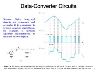
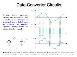
Figure 9.36 The process of periodically sampling an analog signal. (a) Sample-and-hold (S/H) circuit. The switch closes for a small part (t seconds) of every clock period (T). (b) Input signal waveform. (c) Sampling signal (control signal for the switch). (d) Output signal (to be fed to A/D converter). Microelectronic Circuits - Fifth Edition Sedra/Smith
Figure 9.37 The A/D and D/A converters as circuit blocks. Microelectronic Circuits - Fifth Edition Sedra/Smith
Figure 9.38 The analog samples at the output of a D/A converter are usually fed to a sample-and-hold circuit to obtain the staircase waveform shown. This waveform can then be filtered to obtain the smooth waveform, shown in color. The time delay usually introduced by the filter is not shown. Microelectronic Circuits - Fifth Edition Sedra/Smith
Figure 9.39 An N-bit D/A converter using a binary-weighted resistive ladder network. Microelectronic Circuits - Fifth Edition Sedra/Smith
Figure 9.40 The basic circuit configuration of a DAC utilizing an R-2R ladder network. Microelectronic Circuits - Fifth Edition Sedra/Smith
Figure 9.41 A practical circuit implementation of a DAC utilizing an R-2R ladder network. Microelectronic Circuits - Fifth Edition Sedra/Smith
Figure 9.42 Circuit implementation of switch Sm in the DAC of Fig. 9.41. In a BiCMOS technology, Qms and Qmr can be implemented using MOSFETs, thus avoiding the inaccuracy caused by the base current of BJTs. Microelectronic Circuits - Fifth Edition Sedra/Smith
Figure 9.43 A simple feedback-type A/D converter. Microelectronic Circuits - Fifth Edition Sedra/Smith