Download
1 / 15
150 likes | 284 Views
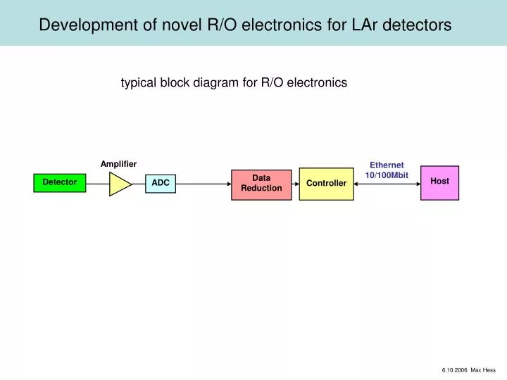
Development of novel R/O electronics for LAr detectors. typical block diagram for R/O electronics. Amplifier. Et hernet 10/100Mbit. Host. Controller. Data Reduction. Detector. ADC. 6.10.2006 Max Hess. + -. 4 FET‘s in parallel. C D. R I. ADC. C I. R D. C F = 1 pF. V ADC.

E N D
Development of novel R/O electronics for LAr detectors typical block diagram for R/O electronics Amplifier Ethernet 10/100Mbit Host Controller Data Reduction Detector ADC 6.10.2006 Max Hess
+ - 4 FET‘s in parallel CD RI ADC CI RD CF= 1 pF VADC Gain = 40 mV/fC RICI = 0.6 s Noise = 2.1 mV rms RF= 470 M RDCD = 1.8 s Shaper Charge amplifier VADC input signal: 200 nA 50 ns = 10 fC Preamplifier for Dark Matter Experiment (ETHZ) Detector: 2 stages LEM ( Large Electron Multiplier ) LEM Gain = 100 / stage 1 electron produce a Q nom =1041.6 10-19C = 1.6 fC 6.10.2006 Max Hess
Argon TubeSignal pulse width & charge in one pad in function from the trace angle • Pad dimensions: 10 mm x 10 mm • vdrift = 2 mm/µs @ Edrift = 1 kV/cm • LEM Gain = 100 • 1 MIP produces 6000 e-/mm in LAr • Qnom = 100 6000 1.6 10-19C = 100 fC/mm p = 10 mm pad vdrift d pulse width: tp = d / vdrift = p / (vdrift cot ) s signal charge: QS = Qnom p s = Qnomp / cos trace signal current: IS = QS/ tp 6.10.2006 Max Hess
Values for simulation p = 10 mm pad vdrift d s * theoretical: tp 0 and IS ∞ trace 6.10.2006 Max Hess
+ - VADC input signal: 2 uA / 50 ns VADC input signal: 20 nA / 10 s Preamplifier for Argon Tube 1 FET VADC Gain = 5.3 mV/nA Noise = 400 V rms CD RI ADC CI RD RF= 1 M RICI = 0.7 s CF=0.1pF RDCD = 1 ms Amplifier with lo- and hi-pass filter Transimpedance Amplifier 6.10.2006 Max Hess
+ - + - Preamplifier for Argon Tube with Op Amp VADC Op Amp AD8655 Gain = 3.5 mV/nA Noise = 860 V rms R1 ADC C1 R2 RF= 330 k VADC C2 R1C2 = 0.7 s R2C2 = 0.7 s CF = 2.2pF input signal: 2 uA / 50 ns Transimpedance Amplifier Linear Amplifier with BW limiting VADC input signal: 20 nA / 10 s 6.10.2006 Max Hess
8 front-end boards DAQ box MUX ADC Ethernet 10/100Mbit 256 channels Host Embeded PC Data Reduction ADC 32 channels ADC Clock module one for all DAQ system other DAQ subsystems 8 Serial links length max. 10 meter 19“ case electrically isolated Flat cables from detector shortest possible: - cable capacitance - noise from outside System ground inside the detector Block diagram for R/O electronics 6.10.2006 Max Hess
Front-end board MUX: 32 ADC channels + 1 channel for status 1 MUX 12 12 CODER: create DC-balanced signal code ( 3 4B5B-code) ADC SHIFT REG REG DS92LV16 32 channels 12 16 CODER SERIALIZER 1 12 12 to DAQ ADC SHIFT REG REG (12) 720 Mb/s CONTROL LOGIC CS* (16) DE-SERIALIZER sclk rclk : 2 from DAQ FPGA Altera EP1C3T144C8 electrically isolated CS*: ADC conversion start(1MS/s) sclk: sample clock = 20 MHz rclk: Readout clock = 40 MHz Preamplifier modules interchangeable for LArDM, ArgonTube, etc. 6.10.2006 Max Hess
Front-end board 32 ADC‘s ADC121S101 Resolution: 12 bit Sample rate: 1 MS/s Full scale: 3.2 V 2 amplifier / print input connector for 32 channels (68 pole flat cable) Multiplexer FPGA Altera EP1C3T144C8 100 mm Serializer/Deserializer NS DS92LV16 Ethernet connector serial link to DAQ board 6.10.2006 Max Hess
Front-end case Ethernet connector serial link to DAQ board 8 Front-End modules = 256 channels / case input connector for 32 channels (68 pole flat cable) 3 HE = 133 mm 6.10.2006 Max Hess
Data reduction INPUT MEMORY DS92LV16 16 16 16 DE-SERIALIZER INPUT FIFO OUTPUT FIFO rclk BUS to Embeded PC and other data reduction boards from Front-end FPGA slow control circular buffer logic for input memory signal comparator data reduction logic from input memory to output FIFO watch for time stamp generation 720 Mb/s SERIALIZER signal detect out to Front-end ext. trigger in EXTERNAL CLOCK MODULE one for all DAQ system watch clock CS* rclk rclk: Readout clock = 2 x ADC clock CS*: ADC conversion start 6.10.2006 Max Hess
Block diagram for data reduction (draft) INPUT BUFFER (SRAM) each channel use 1 circular buffer with 2 sectors = 2 x 4096 x 16 bit total used memory = 4 Mb with tacc < 12ns it‘s possible to write 32 words and read 48 words in 1µs CLOCK 80 MHz 18 16 16 DATA REDUCTION LOGIC INPUT FIFO DELAY FIFO from serial link DATA 16 OUTPUT FIFO (DRAM) 16 B A-B A bus to embeded PC COMP MUX MEMORY CONTROLLER THRESHOLD SIGNAL DET. OUT READ ADDRESS COUNTER WRITE ADDRESS COUNTER addr TRIGGER DELAY COUNTER I / O CONTROLLER TRIGGER ADDRESS FIFO WATCH (resolution 1us) EXTERN TRIGGER INPUT : Altera Cyclone FPGAfamily to serial link, slow control 6.10.2006 Max Hess
Organisation of input buffer one independend circular buffer for each channel with two sectors = 2 x 4096 x 16 bit SD: signal detected read address pointer sector A pre trigger time SD write address pointer sector B 6.10.2006 Max Hess
Frame digital comparator threshold npre npost npre npost t3 Data reduction by frame building Frame 1 Frame 2 digital comparator threshold npre npost npost npre absolute time t1 t2 n samples over threshold registration of possible data during 4095 s = 4095 samples 6.10.2006 Max Hess
Ethernet 10/100Mbit Summary Actual design: - High flexibility for signal conditioning - The system is adaptable for different event rates, variable number of data reduction boards per embeded PC - Optimized for development time to price per channel (for small systems) Front-end modul DAQ box amplifier ADC serial link serial link data reduction embeded PC Future design: Higher number of channels per board Lower power consumption Lower price per channel up to 100‘000 - ASIC Amplifier - ADC with higher sample rate Better time resolution (if needed) Longer possible distance from the detector to the DAQ electronic Higher bandwidth - Optical link Data reduction logic and embeded processor in the same FPGA ( Altera Stratix, Cyclone familly) - DAQ Logic 6.10.2006 Max Hess