Download
1 / 24
390 likes | 744 Views
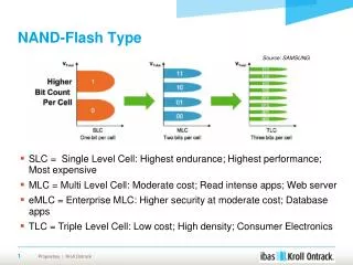
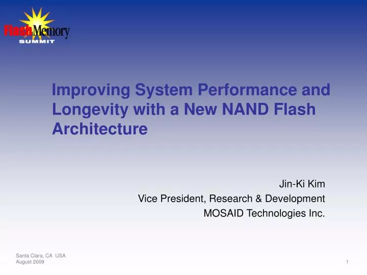
Improving System Performance and Longevity with a New NAND Flash Architecture. Jin-Ki Kim Vice President, Research & Development MOSAID Technologies Inc. Agenda. Context Core Architecture Innovation High Performance Interface Summary. Computing Storage Hierarchy.

E N D
Improving System Performance and Longevity with a New NAND Flash Architecture Jin-Ki Kim Vice President, Research & Development MOSAID Technologies Inc.
Agenda • Context • Core Architecture Innovation • High Performance Interface • Summary
Computing Storage Hierarchy Historical Storage Hierarchy New Storage Hierarchy * SCM: Storage Class Memory R.Freitas and W.Wilcke, “Storage-class memory: The next storage system technology”, IBM J. RES. & DEV. VOL. 52 NO. 4/5 JULY/SEPTEMBER 2008.
32Gb MLC 16Gb MLC 8Gb MLC 4Gb MLC 2Gb SLC 1Gb SLC NAND Flash Progression Density The single-minded focus on bit density improvements has brought Flash technology to current multi-Gb NAND devices 120nm 90nm 73nm 65nm 51nm 35nm Process Technology
1 2 4 A: # of Bit / Cell 1 2 4 B: # of Bitline / Page Buffer 8 16 32 64 C: # of Cell / NAND String 512B 2KB 4KB 8KB 16KB D: Page Size Block Size = (A * B * C) * D Cell Array Mismatch Factor (CAMF) NAND Architecture Trend • Primary focus is density for cost and market adoption
NAND Block Size Trend Cell Array Mismatch Factor (CAMF) is a key parameter to degrade write efficiency (i.e. increase write amplification factor) CAMF = 128 (SLC) & 256(MLC) CAMF = 64 (SLC) & 128(MLC) CAMF = 32 CAMF = 16 CAMF = 8
NAND Challenges in Computing Apps • Endurance: 100K 10K 5K 3K 1K • Retention: 10 years 5 years 2.5 years • Current NAND architecture trend accelerates reliability degradation
Write Efficiency = Total Data Written by Host Total Data Written to NAND System Lifetime = Total Host Writes Host Writes per Day Flash System Lifetime Metric • System lifetime heavily relies on NAND architecture and features, primarily cell array mismatch factor Total Host Writes = NAND Endurance Cycle * System Capacity * Write Efficiency * Wear Leveling Efficiency
NAND Architecture Innovation Current NAND Flash Architecture Plane 2 Plane 1 Page Buffer: 512B 2K 4KB 8KB
NAND Architecture Innovation FlexPlane with 2-tier Row Decoder Scheme • Smaller & Flexible Page Size (2KB/4KB/6KB/8KB) • Smaller & Flexible Erase Size • Lower power consumption due to segmented pp-well FlexPlane Global Row Decoder NAND Cell Array on Sub PP-Well NAND Cell Array on Sub PP-Well NAND Cell Array on Sub PP-Well NAND Cell Array on Sub PP-Well Segment Row Decoder Segment Row Decoder Segment Row Decoder Segment Row Decoder 2KB Page Buffer 2KB Page Buffer 2KB Page Buffer 2KB Page Buffer FlexPlane Operations
NAND Architecture Innovation2-Dimensional Page Buffer Scheme Upper Plane 2-Dimensional Page Buffer (Shared Page Buffer) 0.5x Bitline Length compared to conventional NAND architecture Lower Plane Micron 32Gb NAND Flash in 34nm, 2009 ISSCC
Block Erase Partial Block Erase Page-pair Erase NAND Core InnovationPage-pair & Partial Block Erase • Minimize cell array mismatch factor • Improve write efficiency • MOSAID’s Erase Scheme
NAND Core InnovationLower Operating Voltage 2.7 ~ 3.3V 3.3V 2.7 ~ 3.3V H.V. Gen H.V. Gen H.V. Gen 1.8V Core and Peri. Core and Peri. Core and Peri. 1.8V I/O I/O I/O • MOSAID’s Low Stress Program Scheme
NAND Core InnovationLow Stress Program • Precharge NAND string to voltage higher than Vcc prior to wordline boost and bitline data load • Reduces program stress (Vpgm & Vpass stress) during programming • Eliminates Vcc dependency to achieve low Vcc operation • Minimizes background data dependency • Eliminates W/L to SSL Coupling • Addresses Gate Induced Drain Leakage (GIDL)
HyperLink (HLNAND™) Flash Monolithic HLNAND MCP HLNAND
HLNAND HLNAND Host Controller Interface HLNAND HLNAND HyperLink Interface • Point-to-point ring topology • Synchronous DDR signaling with source termination only • Up to 255 devices in a ring without speed degradation • Dynamically configurable bus width from 1-8 bits • HL1 parallel clock distribution to 266MB/s • HL2 source synchronous clocking to 800MB/s, backward compatible to HL1
32Gb SLC/64Gb MLC HLNAND MCP • HL1 (DDR-200/266) using NAND in MCP - Conform SLC/MLC HLNAND spec 8Gb SLC/16Gb MCL HLNAND Bridge Chip developed by MOSAID and implemented in a MCP
32Gb SLC/64Gb MLC HLNAND MCPMCP Package – 12 x 18 100-Ball BGA
32Gb SLC/64Gb MLC HLNAND MCPPerformance DDR Output Timing (Oscilloscope Signals) – will be inserted DDR-300 Operations 151MHz (tCK = 6.6ns) @Vcc = 1.8V
HLNAND Flash Module (HLDIMM) • Use cost effective DDR2 SDRAM 200-pin SO-DIMM form factor and sockets • 8 x 64Gb or 8 x 128Gb HLNAND MCP (4 on each side)
HL1 MCP HL1 MCP HL1 MCP HL1 MCP HL1 MCP HL1 MCP HL1 MCP HL1 MCP HLDIMM Port Configuration • 2 x HyperLink HL1 interfaces with 533MB/s read + 533MB/s write = 1066MB/s aggregate throughput front back Pin 1 Pin 2 CH0 in CH0 out CH0 out CH0 in to controller next HLDIMM CH1 in CH1 out CH1 out CH1 in HLDIMM Pin 200 Pin 199
1066MB/s Aggregate Throughput 2133MB/s Aggregate Throughput System Configurations with HLDIMM
Summary • The driving forces in future NVM are the memory architecture & feature innovation that will support emerging system architectures and applications • Using HLNAND Flash, Storage Class Memory is viable today using proven HLNAND flash technology
Resource for HLNAND Flashwww.HLNAND.com • Available • 64Gb MLC MCP sample • 64GB HLDIMM sample • Architectural Specification • Datasheets • White papers • Technical papers • Verilog Behavioral model