Download
1 / 50
500 likes | 513 Views
Dive into the world of transistors, from the basics of silicon doping and P-N junctions to advanced transistorized technologies. Learn how these tiny components revolutionized electronics. Discover how transistors replaced vacuum tubes, enabling compact and efficient devices.

E N D
Relay Vacuum Tube and CRT Thermometer using Thermistor Old Zenith Radio Individual Transistor Integrated Circuit (IC) Video: Transitorized
From Silicon to Transistor What is Silicon Doping Silicon A P-N Junction The Diode The LED (Light Emitting Diode) How does a Transistor work The Bipolar Transistor The Field Effect Transistor Benefits of using transistors Able to amplify an alternating signal Used as a fast switch Low Power Solid state and small in size Inexpensive First uses of Transitors Replaced Vacuum tubes in radios and computers Hearing Aids Airplanes 4004 – First single chip Microprocessor where transistors are integrated on a single piece of Silicon
A semiconductor is a material that in it pure form does not conduct electricity well. Silicon is a common semiconductor. It makes up 25% of the earth’s crust. Only Oxygen is more abundant than Si. A silicon atom shares electrons with four neighboring Si atoms allowing the outer shell to be filled completely. http://www.thenakedscientists.com
A small amount of energy knocks electrons from bonds In Pure Silicon, # of Electrons = # of Holes Electron-Hole Pair is produced when this happens.
A Semiconductor can be used to measure Temperature Conductivity increases rapidly as temperature rises.
Properties of Silicon can be modified Contaminants can be added (1 part per 10 million) These contaminants are called Dopant Dopants change the electrical properties of Silicon Both types of charge carriers can be added to Silicon (positive and negative Charge Carriers are Electrons and Holes
By substituting some of the Silicon with atoms that have five (instead of four) outer electrons, there are electrons left over to roam (1 per Dopant atom). • By substituting some of the Silicon with atoms that have three outer electrons ‘holes’ are created (1 per Dopant atom). Negatively doped Silicon Positively doped Silicon
P-type Dopant N-type Dopant
Diode is a p-n junction • Diode is a one-way electrical switch that passes current in one direction only. • Constructed with a semiconductor • Our Radio uses a Germanium Diode
Electrons and Holes pushed toward junction when a positive voltage is applied to the p-side
When negative voltage is applied to p-side, Electrons and Holes are swept away from the junction, so no current flows in circuit
With an LED, light energy is given off when an electron and hole recombine. A roaming electron has more energy than an electron bound to an atom
Converting sunlight directly into DC electricity using Photovoltaics (PV): • Sunlight hits a sandwich of doped silicon. Electrons are knocked out of their orbits. • The electron flow provides the current, and the cell's electric field produces a voltage. PV was developed In the 1950’s for Powering Satellites.
How do Photovoltaics (PV) work? • A is n-type Si (e.g. Phosphorus) • B is p-type Si (e.g. Boron)
P-Type dopants N-Type dopants
E-field Just at the junction the electrons and holes mix, creating a an electric field (voltage) separating the two sides. This voltage allows electrons to flow up but resists electrons flowing down. The solar cell is a large diode; current flows in one direction only.
Light frees electrons creating Electrons and Holes http://www.specmat.com/Solar%20Cell%20Description.jpg
A – glass coating B – contact grid C – Antireflective coating D – N-type Si E – P-type Si http://www.specmat.com
PV System with Batteries http://www.wcubed.com/solar/solar_photovoltaics.htm
What is a Transistor Made of doped semiconductor materials, the transistor is used to amplify electrical signals or used as a switch. http://fourier.eng.hmc.edu
The Diode Reverse Biased:Electrons and holes swept away from the junction, so no current flows in the circuit.
The Bipolar NPN Transistor The base-emitter junction is forward biased, the base-collector junction is reverse biased. The transistor is bipolar because both charge carriers (holes and electrons) are present.
By doping (adding impurities to) a semiconductor material (i.e. Silicon or Germanium), very different electrical properties are created. • By sandwiching these dissimilar materials, a transistor is made. • If the base is thin, electrons from the emitter are swept though the base to the collector. Electrons in the collector then respond to the positive voltage and flow out of the collector.
Basic Amplifier Circuit using the NPN Bipolar Transistor http://www.tpub.com
Model of first Transistor c. 1947 http://www.porticus.org/bell
Fabricating a transistor on a single piece of doped silicon wikipedia CNN.com
The Field Effect Transistor (FET) Electricity flows from the Source to the Drain when an electric field is applied to the Gate.
Field Effect Transistor (FET) FETs are tiny switches that can open and close very quickly. A negative voltage will turn this p-channel transistor on. ‘On’ means there is a connection between the Source and Drain. http://www.answers.com
Before the transistor, there was the Vacuum Tube • Also used to amplify signals • Also used as a switch
http://www.privateline.com Electrons are “boiled” off the cathode and attracted to the anode because of the applied voltage. A grid controls the electron flow. The signal to be amplified is connected to the grid. A small signal controls a much larger voltage.
Cathode Ray Tube (CRT)Still is use Today Vacuum Tube, Electron Gun, Fluorescent Screen, and Coils which accelerate and deflect the electron beam
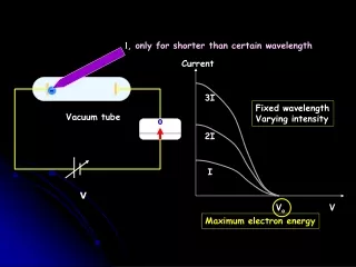
Prior to Vacuum tube: • No coast-to-coast telephone calls • Wireless Telegraph in use – Morse codes received and boosted using relays. • Alternating Signals could not be amplified with relays • Signals were sent over wires no farther than NY to Denver Relay: switch that opens and closes and is controlled by current in another circuit. Two settings: OPEN And CLOSED
http://www.porthcurno.org.uk/html/morsecircuit.html On or Off, current is either constant or it does not flow. Applying a small varying signal (voice signal) here would not produce a varying signal in the top circuit.
AT&T interested in the Transistor • Vacuum Tubes were unreliable for amplifying signals in transcontinental telephone calls. • Vacuum Tubes consumed a lot of power and got hot. • Competition from other phone companies made reliable and fast phone service important. • Expensive, bulky, and fragile.
ENIAC in 1946 First electronic computer Designed for the Army $500,000 >17,000 Vacuum Tubes 150 KW of power Filled multiple rooms (700 sq. ft) Soldered and constructed by hand by the University of Penn.
Hearing Aids - the first commercial devices that used transistorsc. 1953 http://blog.modernmechanix.com
Some Hearing Aids do not amplify sound:Cochlear Implants bypass portion of the ear that is damaged Cochlear Nerve sends auditory information to the brain. Wikipedia
Cochlear Implant Components • Electrode Array • Receiver • Speech Processor • Transmitting Coil • Microphone http://deafblind.com/cochlear.html
Individual Parts Integration of parts required hand wiring Early Sony Transistor Radio
The birth of the integrated circuit (IC) • 1947- using silicon as a transistor is discovered • 1959- Texas Instruments put 10 transistors on one piece of silicon. First company to use Silicon instead of Germanium • Used in Apollo Program to achieve moon landing – transistors integrated on pieces of silicon offered lower power and weight. 1961-69
Intel 4004 The World’s first Microprocessor, made in 1971 Computer on a chip! It had 2300 transistors and ran at 740 KHz. It could execute 45 instructions. Could execute 96,000 instructions per second As powerful as the ENIAC
Chips can have billions of transistors built on a small piece of silicon. CMOS stands for ‘Complimentary Metal Oxide Semiconductor’. This means CMOS chips contain both pMOS and nMOS transistors. http://www.britannica.com
Sources http://www.pbs.org/transistor/


![What is an IC ? [integrated circuit]](https://cdn1.slideserve.com/2972450/slide1-dt.jpg)