Download
1 / 8
120 likes | 546 Views
Process and Material Properties Of PECVD Boron-Doped Amorphous silicon Film. Abstract Authors: Helinda Nominanda and Yue Kuo. Presented by Chakravarthy. Thin Film Microelectronics Research Laboratory Department of Chemical Engineering Texas A&M University,College Station,TX.

E N D
Process and Material Properties Of PECVD Boron-Doped Amorphous silicon Film. Abstract Authors: Helinda Nominanda and Yue Kuo. Presented by Chakravarthy
Thin Film Microelectronics Research LaboratoryDepartment of Chemical EngineeringTexas A&M University,College Station,TX.
The effect of temperature and dopant gas flow on PECVD boron-doped amorphous silicon film properties such as deposition rate and resistivity were studied.
Deposition Process. • Films were deposited at 50 KHz using a cold wall reactor with horizontal electrodes. • A 2000 Angstrom thick PECVD silicon nitride film was deposited on a glass substrate as an adhesion layer. • Temperature of 100-300 degree Celcius • 40-200 sccm of diborane + 400 sccm of hydrogen +35 sccm silane(99.999%) • Pressure at 0.25 Torr • Power density of 205 mW/sq.cm.
*The substrate temperature has a more pronounced effect on the deposition rate than the dopant gas flow rate.
*Resistivity decreases with temperature. *A more uniform resistivity is achieved at higher temperatures.
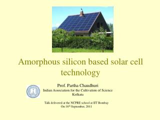
Applications of PECVD Amorphous Silicon Films. • TFT arrays of active matrix liquid crystal display(AMLCDs) • p-I-n junction capacitors • Solar cells and Optoelectronic devices.
Summary Deposition parameters have huge impact on the material properties of the PECVD boron-doped amorphous silicon films.