Download
1 / 10
100 likes | 291 Views
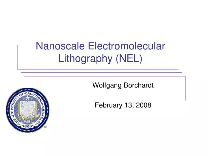
Nanoscale Electromolecular Lithography (NEL). Wolfgang Borchardt February 13, 2008. Short Introduction to NEL. New technique , proposed in 2005 by W. Shen , Y. Chen and Q. Pei (UCLA) Nanoscale patterning of resists by using an electric mask

E N D
Nanoscale Electromolecular Lithography (NEL) Wolfgang Borchardt February 13, 2008
Short Introduction to NEL • New technique, proposed in 2005 byW. Shen, Y. Chen and Q. Pei (UCLA) • Nanoscale patterning of resists by using an electric mask • mask: metal patterns on an insulative substrate (e.g. glass) • Nanoscalemetal patterns fabricated by e-beam and optical lithography or self-assembly • electrochemicalpolymerizationin a water solution with 0.2 M pyrrole monomers and 0.15 M KCl • voltage pulse with an amplitude of +1.0 V and a duration of 60 s • Sources: • NSF Nanoscale Science and Engineering Grantees Conference, Dec 12-15, 2005 • Nanoscale Electromolecular Lithography (NEL) by Yong Chen… • APPLIED PHYSICS LETTERS 87, 124106 2005 • Electric lithography by electrochemical polymerization by W. Shen,Y. Chen and Q. Pei, UCLA Wolfgang Borchardt
1st step Electrode Mask Insulator Resist Electrode Substrate Wolfgang Borchardt
2nd step Electrode Insulator Electrode Wolfgang Borchardt
3rd step Wolfgang Borchardt
4th step Wolfgang Borchardt
Results Left: SEM image of nanowire patterns Right: AFM image of nano dot patterns a) Linearly patterned mask b) Selectively transferred lines c) AFM image: constant voltage applied with different durations Wolfgang Borchardt
Sub-10nm resolution? Twoclassesofresists • Traditional Self-assembledmonolayers(SAMs): Reengineering: • exposure of useful chemical functional groups • topographical changes • Highly crosslinked 2D-arrays: • self-assembledontoelectrodesurfacesinto simple patterns • EC-field will break crosslinks • „Carving out“ of nanometer-scale regions Wolfgang Borchardt
Advantages / Disadvantages + High-throughput => mass production + Scalable + Reliable / robust + Reduced defect density and improved yield in comparison with the 3D mold and mechanical process used in nanoscale imprint lithography - Low resolution (>300nm) until now - Nobody else reporting on this topic Wolfgang Borchardt
Questions Wolfgang Borchardt