Download
1 / 27
280 likes | 302 Views
Explore an FPGA platform for rapid data acquisition with high spatial & time resolution for various scientific applications such as medical diagnostics and materials research. The system requires a high-granularity, low-noise detector and high readout bandwidth for real-time data processing.

E N D
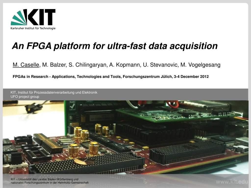
An FPGA platform for ultra-fast data acquisition M. Caselle, M. Balzer, S. Chilingaryan, A. Kopmann, U. Stevanovic, M. Vogelgesang FPGAs in Research - Applications, Technologies and Tools, Forschungszentrum Jülich, 3-4 December 2012
Ultra Fast X-ray Imaging (ANKA/UFO experimental station) UFO Ultra-Fast X-ray Imaging of Scientific Processes with On-line Assessment and Data-driven Process Control High spatial resolution (<1 µm) included 2D and 3D visualizations + Time resolution (2D: ≈10kHz, 3D: ≈10Hz) to give insight in the temporal structure evolution and thus access to dynamics of processes Main application fields: medical diagnostics, biology, non-destructive testing, materials research and etc. Requirements: High granularity and low noise monolithic silicon pixel detector, few µm pixel pitch, several MPixel matrix operating at several kframes/sec High readout bandwidth up to 50Gb/s with GPU (3D-tomography reconstruction) FPGAs in Research - Applications, Technologies and Tools, Forschungszentrum Jülich, 3-4 December 2012. M. Caselle
KIT-IPE – Readout concept of high data throughput for scientific applications Real time data elaboration Data reduction High-throughput data flow DAQ Boards Concept: Data source GPUs/CPUs infrastructure Up to 10GB/s Up to 4 GB/s FPGA Memory FPGA FPGA Up to 0.25 GB/s X-ray detector CMOS image sensor Fast ADC …. Input stage Input stage Connection High speed Driver Driver High speed Small PCIe backplane Memory Memory GPU/CPU algorithms GPU/CPU algorithms Feedback loops Connection Data storage LSDF Under developing by Data processing group in KIT-IPE Fast Data storage Fast Data storage FPGAs in Research - Applications, Technologies and Tools, Forschungszentrum Jülich, 3-4 December 2012. M. Caselle
KIT-IPE – Readout concept of high data throughput for scientific applications Real time data elaboration Data reduction High-throughput data flow DAQ Boards Concept: Data source GPUs/CPUs infrastructure Up to 10GB/s Up to 4 GB/s FPGA Memory FPGA FPGA Up to 0.25 GB/s X-ray detector CMOS image sensor Fast ADC …. Input stage Connection Input stage High speed Driver Driver High speed Small PCIe backplane Memory Memory GPU/CPU algorithms GPU/CPU algorithms Feedback loops Connection Data storage LSDF Implementation: Under developing by Data processing group in KIT-IPE Fast Data storage Fast Data storage Daughter sensor board FPGA Virtex 6 UFO Camera Mother readout board This talk is focus on FPGA & Readout Board PCIe link to DAQ Small backplane FPGAs in Research - Applications, Technologies and Tools, Forschungszentrum Jülich, 3-4 December 2012. M. Caselle
Flexible high-throughput FPGA platform FPGA internal architecture PC DAQ 4 X lanes @ 500Mbit/s CPU FSM Master control Data Source (Detector) SerDes input stage (KIT_ipcore) FIFO Chipset root port Optical/Electrical X4 lanes @ 5Gb/s ... User bank register Detector Control memory memory memory 4 Remote Detector Control FPGAs in Research - Applications, Technologies and Tools, Forschungszentrum Jülich, 3-4 December 2012. M. Caselle
Flexible high-throughput FPGA platform FPGA internal architecture PC DAQ 4 X lanes @ 500Mbit/s CPU FSM Master control Data Source (Detector) SerDes input stage (KIT_ipcore) FIFO Chipset root port On-line parallel data processing Optical/Electrical X4 lanes @ 5Gb/s ... User bank register Detector Control memory DDR interface (KIT_ipcore) memory memory 4 DDR3 memory (800MHz @ 64bit) Remote Detector Control FPGAs in Research - Applications, Technologies and Tools, Forschungszentrum Jülich, 3-4 December 2012. M. Caselle
Flexible high-throughput FPGA platform FPGA internal architecture PC DAQ 4 X lanes @ 500Mbit/s PCI Express + DMA (KIT_ipcore) CPU FIFO FSM Master control Data Source (Detector) SerDes input stage (KIT_ipcore) FIFO Chipset root port FIFO On-line parallel data processing Optical/Electrical X4 lanes @ 5Gb/s ... User bank register Detector Control memory DDR interface (KIT_ipcore) memory memory 4 Virtex6 - floorplan DDR3 memory (800MHz @ 64bit) Remote Detector Control DDR3 interface • Three logic cores have been developed for a flexible high-throughput platform • PCIe-Bus Master DMA readout architecture PCIe • Multi-port high speed DDR3 interface • Configurable 2..16 bits “SerDes” (Serializers /Deserializers) architecture SerDes & input stage • PCI Express/DMA Linux 32-64 bits driver with ring buffer data management DMA • Integration in the parallel GPU/CPU computing framework FPGAs in Research - Applications, Technologies and Tools, Forschungszentrum Jülich, 3-4 December 2012. M. Caselle
PCIe-Bus Master DMA readout architecture FPGA core DMA driver GTX Transceivers X8 @ 5Gb/s Xilinx Integrated block for PCI Express GEN 2 Custom PCIe – DMA Interface I/O interface logic Data out [0..63] 4 Data decoding and consistency check DMA Engines NW Data valid GPU/CPU Applications OUT port Busy_logic Clock_out FIFO Optical/Electrical X4 lanes @ 5Gb/s I/O interface logic RD - Control packet FSMs Data in [0..63] WR - Control packet FSMs FIFO WR_EN IN port Xilinx / North-West IP-core Back-pressure Clock_in 4 • Bus Master DMA operating with 4lanes PCIe @ Gen2 (250MHz) User bank register FPGA temp. & voltage control Software layers User applications • Two individual engines for write/read from FPGA (User logic) to PC centre memory • IN and OUT FIFO-like interface (for User logic) • FIFO used to decouple the time domain between DMA and User custom logic FPGAs in Research - Applications, Technologies and Tools, Forschungszentrum Jülich, 3-4 December 2012. M. Caselle
Preliminary, PCIe-Bus Master DMA new architecture Disadvantage of IP-cores from external vendors, are: 1) expensive (35k€ for North-West DMA and 10-60k€ for EZDMA/QuickPCIe-IP by PLDA) 2) for unique FPGA family (Virtex 6, speed grade -2) FPGAs in Research - Applications, Technologies and Tools, Forschungszentrum Jülich, 3-4 December 2012. M. Caselle
Preliminary, PCIe-Bus Master DMA new architecture Disadvantage of IP-cores from external vendors, are: 1) expensive (35k€ for North-West DMA and 10-60k€ for EZDMA/QuickPCIe-IP by PLDA) 2) for unique FPGA family (Virtex 6, speed grade -2) New, KIT-IPE Bus Master DMA engines operating with x8 lanes PCI Express @ GEN 2 IN/OUT data at 128 bit @ 250MHz internal bandwidth of 32 Gb/s in Read/Write Virtex6 - floorplan FPGA resource estimation < 4% RX engine TX engine Preliminary Data valid for X58 PCIe chipset FPGA ring buffer management on-going PCIexpress GEN2 Software 64bit@linux driver under optimization (~ 32Gb/s) FPGAs in Research - Applications, Technologies and Tools, Forschungszentrum Jülich, 3-4 December 2012. M. Caselle
Two-ports DDR3 memory interface architecture Why a two-ports DDR3 memory controller .. ? The Xilinx Multi-port Memory Controller (IP-Core) is limited in the maximum data throughput (less than 2GB/s for each port) & complex user interface. Ref. LogiCORE IP Multi-Port Memory Controller (MPMC) (v6.03.a), DS643 March 1, 2011 FPGAs in Research - Applications, Technologies and Tools, Forschungszentrum Jülich, 3-4 December 2012. M. Caselle
Two-ports DDR3 memory interface architecture Why a two-ports DDR3 memory controller .. ? The Xilinx Multi-port Memory Controller (IP-Core) is limited in the maximum data throughput (less than 2GB/s for each port) & complex user interface. Ref. LogiCORE IP Multi-Port Memory Controller (MPMC) (v6.03.a), DS643 March 1, 2011 PHY- DDR Xilinx IPCore Data_in [0..N] WR FIFO 256bit @200 MHz WR_EN Data frame segment Clock_in Start address Port 1 WR DDR FSM DDR3 Memory Arbiter FSM Start address Port 2 User Control Interface (800MHz @ 64 bit) Read/Write RD DDR FSM DDR Busy On-line data process segment RD FIFO Data_out [0..M] 256bit @200 MHz Data_valid Clock_out • Bandwidth 51Gb/s, limited by FPGA speed grade ( Virtex 6, speed grade -1) • Two operations are possible in same/different segmentation/s (each operation ~ 25Gb/s) • Data interface FIFO-like, minimum control signals are required • FIFO used to decouple the time domain between Memory Controller and custom User logic • Configurable user define data width N and M 32/64/128/512 bits FPGAs in Research - Applications, Technologies and Tools, Forschungszentrum Jülich, 3-4 December 2012. M. Caselle
A configurable “SerDes” input stage architecture Why not a Xilinx ISERDERSE stage .. ? Limited parallel data width (output) not more than 10bits (for two ISEDERSE in cascade configuration) and not dynamically configurable. The FSM Alignment in not included in the Xilinx tools. Ref. Virtex-6 FPGA Select IO resources user guide. ug361 (v1.3) august 16, 2010. FPGAs in Research - Applications, Technologies and Tools, Forschungszentrum Jülich, 3-4 December 2012. M. Caselle
A configurable “SerDes” input stage architecture Why not a Xilinx ISERDERSE stage .. ? Parallel data output IBUF Limited parallel data width (output) not more than 10bits (for two ISEDERSE in cascade configuration) and not dynamically configurable. The FSM Alignment in not included in the Xilinx tools. IODELAY Custom SerDes logic Serial data Ref. Virtex-6 FPGA Select IO resources user guide. ug361 (v1.3) august 16, 2010. Data (PAD) Bit-slip IDDR Configurable 2 to 16bit parallel data output “SerDes “ logic with MSB Alignment State Machine I/O clock Buffer IBUF 1 0 1 1 0 0 1 0 + + 10110010 IDDR - - Alignment FSM Clock Data lock Clock (PAD) Regional clock buffer From CMOS sensor or FADC, etc. Regional Clock Serial/parallel and FSM Alignment Clock division Clock to Data Time tuning Training pattern Parallel data width Clock Buffer I/O FPGA user defined Data CLOCK • Individual clock-to-data time tuning by IODELAY (time step of 75psec) • I/O clock buffer located in the centre of the FPGA bank • Regional buffer synchronous to parallel data out • “SerDes” input stage fully configurable by User FPGAs in Research - Applications, Technologies and Tools, Forschungszentrum Jülich, 3-4 December 2012. M. Caselle
Future developments for high speed readout systems Requirements: • Real-time FPGA + GPU data elaboration high data throughput (range of 64Gb/s) • Data source and FPGA readout board located far from DAQ system • Using commercial/well-known protocol for ease interface with commercial devices/boards Two differents approaches are possible: • Peer – to – peer (P2P) streaming data transfer (based on new generation of PCI express protocol) • Point– to – node (net) for distributed GPU/CPU High Performance Computing (HPC) clusters FPGAs in Research - Applications, Technologies and Tools, Forschungszentrum Jülich, 3-4 December 2012. M. Caselle
IPE - PCI Express Readout card - Overview • PCIe GEN3 optical/electrical data transmission (8 lanes x 8GT/s) Readout Board - Concept EndPoint PCIe Integrated block x8 lanes GEN2 DDR3 Memory Multi-port PCIe switching X8 lanes GEN3 FPGA -Virtex 6 PCIe User logic Electrical cable (up to 5m) PCIe To PC host board No DMA is needed Data Source Optical cable (up to 30m) MiniPOD X12 lanes optics cable for PCIe GEN3 (8 GT/s per lane) Size 18.6 mm x 22 mm, height 14.5 mm • 64 Gb/s (W) + 64Gb/s (R) full-duplex mode • FPGA Real Time process close to data source FPGAs in Research - Applications, Technologies and Tools, Forschungszentrum Jülich, 3-4 December 2012. M. Caselle
IPE - PCI Express Host card- Overview • PCIe host board with high speed data recording PCIe – host card NAND flash SSD Up to 2TB @ 64 Gbit/s FPGA SRAM To PC memory system for GPU data elaborations DMA integrated X16 lanes PCIe slot • Fully configurable data flow FPGAs in Research - Applications, Technologies and Tools, Forschungszentrum Jülich, 3-4 December 2012. M. Caselle
High bandwidth readout system based by InfiniBand Optical or electrical data link up to 100m Data Source µ /ATCA FPGA Optionally Input stage QSFP+ 40Gb/s InfiniBand, in house QDR 40Gbps InfiniBand protocol Memory 120Gb/s InfiniBand available soon 384Gb/s in the next two years Ultra-low latency for high cluster performance Infiniband Router 8-port switch capable of up to 640Gb/s InfiniBand DAQ cluster InfiniBand GPU cluster under developing in KIT-IPE by Data processing group IPE-KIT Heterogeneous FPGA + CPU + GPU FPGAs in Research - Applications, Technologies and Tools, Forschungszentrum Jülich, 3-4 December 2012. M. Caselle
InfiniBand readout Board - Overview InfiniBand Readout board DDR3 InfiniHost III Ex InfiniBand silicon device MicroBlaze QSFP + InfiniBand Mellanox User logic InfiniBand switch PCIe QSFP + JTAG for programming and BSDL (VHDL) test CPLD & Flash JTAG Xilinx -Virtex 6 SDRAM From data Source High Speed connectors (HPC Samtec or similar) IP based application layer possible (i.e. TCP, UDP, SSH, FTP .. ) The InfiniHost provide the PHY, Link and Transaction layers for InfiniBand Remote DMA for fast data transfer intranet communication FPGAs in Research - Applications, Technologies and Tools, Forschungszentrum Jülich, 3-4 December 2012. M. Caselle
Conclusion and What’s next • Logic cores for high data throughput platform employed in several scientific applications: • TeraHz detector + readout system for CSR (M.Caselle, V. Judin, A.S. Müller, M. Siegel, N. Smale, P. Thoma, M. Weber, S. Wünsch). KIT departments IPE-IMS and ANKA • A X-ray camera for phase contrast tomography (M. Caselle, A. Kopmann, Felix Beckmann (HZG), Joerg Burmester(HZG) KIT and HZG • A X-ray camera for high spatial resolution tomography (M. Caselle, M. Balzer, A. Kopmann, V. E. Asadchikova) Shubnikov Institute of Crystallography, Russian Academy of Sciences, Moscow, Russia • A readout electronics for Ultrafast electron beam X-ray tomography system "ROFEX“ in HZDR (proposal under discussion) • New KIT-DMA (32Gb/s) engines developed and tested • Driver 64bit@Linux under optimization What’s next • Design & production of readout board based by: • PCIe GEN3 optical communication • InfiniBand protocol • Integration in the GPU/CPU compute infrastructure FPGAs in Research - Applications, Technologies and Tools, Forschungszentrum Jülich, 3-4 December 2012. M. Caselle
Bandwidth: 8 Gb/s. Future upgrade: 50Gb/s UFO-Camera Train 2 Train 1 Thank you for your attention Frame rate from 500 to 2Kfps 2 nsec 184 bunches revolution time 368ns Bandwidth: 6Gb/s: Future upgrade to 24Gb/s Pulse shape (width 200ps) ANKA Train 3 32 samples inside ….. bunch 92 picosec Recording & analysis of time evolution of each bunch in a multi-bunches accelerator filling-scheme Sample time resolution < than 3psec FPGAs in Research - Applications, Technologies and Tools, Forschungszentrum Jülich, 3-4 December 2012. M. Caselle
Backup slides .. FPGAs in Research - Applications, Technologies and Tools, Forschungszentrum Jülich, 3-4 December 2012. M. Caselle
InfiniBand: Link layer Flow Control Credit-based link-level flow control • Link Flow control assures NO packet loss within fabric even in the presence of congestion • Link Receivers grant packet receive buffer space credits per Virtual Lane • Flow control credits are issued in 64 byte units FPGAs in Research - Applications, Technologies and Tools, Forschungszentrum Jülich, 3-4 December 2012. M. Caselle
InfiniBand: application layers and latency UDP or TCP, FTP, ssh … Designing with InfiniBand Ref: Introduction to InfiniBand™ for End Users, InfiniBand Trade Association Administration 3855 SW 153rd Drive Beaverton, OR 97006 Number of node FPGAs in Research - Applications, Technologies and Tools, Forschungszentrum Jülich, 3-4 December 2012. M. Caselle
UFO architecture - overview Smart high-speed camera Data management and distribution GPU server online monitoring and evaluation X-ray beam line Sample set-up Memory Optical link FPGA On-line Processing Post Processing Sample and detector manipulator Data Evaluation Raw Data Processing Fast Data Link Sample Environment Storage Management Processing Visualization Detector Scintillator & optic lens sample Fast HW loop Beamline Large scale data facility (LSDF) Fast-reject Trigger 2D and 3D image-based control loop SW control loops Experimental station • High speed & bandwidth, full programmable camera (continuous data acquisition at full speed) • Optimized image processing algorithm using GPU computing • Fast HW loop: On-line image-based self-event trigger architecture (Fast reject) • SW control loops: based on 2D and 3D data evaluation: 2D data camera calibration, autofocus, self-alignment & etc.. 3D data reconstructed like optical flow, etc FPGAs in Research - Applications, Technologies and Tools, Forschungszentrum Jülich, 3-4 December 2012. M. Caselle
UFO Camera - overview Mother Readout board (ml605) EndPointPCIe link (to UFO infrastructure) Daughter board with CMOSIS sensor Large DDR3 local memory Xilinx FPGA (for fast readout & on-line data process) Peltier cell (camera cooling) Peltier cell control board cture) Heat sink + fan The main features already implemented and tested, include: • Fully configurable camera adjustable image exposure time and dynamic range, analog and digital pixel features as pixel threshold, mask, analog gain, etc. • Continuous data acquisition at full speed • On-line image-based self-event trigger architecture (Fast reject) • Region-of-interest readout strategy using self-event trigger information • Easily extendable to any available CMOS image sensor FPGAs in Research - Applications, Technologies and Tools, Forschungszentrum Jülich, 3-4 December 2012. M. Caselle
Readout electronics for Coherent Synchrotron Radiation Measure of the peak amplitude of each bunch (resolution few mV) Measure of the pulse width of each bunch (resolution few psec) Analog signal (single bunch) (output of amplifier) Measure of the relative time jitter between electron bunches (res. few psec) Strategy: Digitalize each pulse with 4 samples + pulse reconstruction & Constant Fraction Discriminator (CFD) for precise pulse timestamp. Train 2 Train 1 FWHM = 42 ps 20 – 200 mV 2 nsec 184 bunches revolution time 368ns ANKA CSR (long observation time with YBCO) Pulse shape (width 200ps) Train 3 ANKA 32 samples inside ….. bunch 92 picosec Recording & analysis of time evolution of each bunch in a multi-bunches accelerator filling-scheme Sample time resolution < than 3psec FPGAs in Research - Applications, Technologies and Tools, Forschungszentrum Jülich, 3-4 December 2012. M. Caselle