Download
1 / 23
230 likes | 373 Views
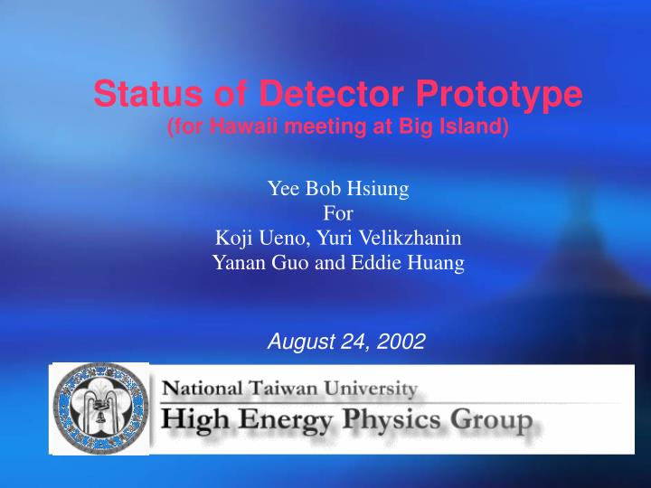
Status of Detector Prototype (for Hawaii meeting at Big Island). Yee Bob Hsiung For Koji Ueno, Yuri Velikzhanin Yanan Guo and Eddie Huang. August 24, 2002. First Simple Prototype. Optical – commercial Fresnel Lens (NTK-F300, f30cm, size=30cm, pitch=0.5mm, PMMA UV), UV filter (BG3)

E N D
Status of Detector Prototype (for Hawaii meeting at Big Island) Yee Bob Hsiung For Koji Ueno, Yuri Velikzhanin Yanan Guo and Eddie Huang August 24, 2002
First Simple Prototype • Optical – commercial Fresnel Lens (NTK-F300, f30cm, size=30cm, pitch=0.5mm, PMMA UV), UV filter (BG3) • MAPMT – Hamamatsu 4x4 (H6568) or 8x8 (H7546) • Readout electronics –Preamp, Receiver, Trigger, ADC and DAQ
Trigger PMT Preamp. Receiver ADC DAQ Readout Setup 64-channels Trigger module VME Freshnell lens UV filter 64-channels Acromag ADC At PC, Visual C++ based Hamamatsu PMT 8x8 or 4x4 1 or 4 16-channels preamplifiers 2 or 8 8-channels receivers
Hamamatsu MAPMT test Anode Uniformity of different channels Data from Hamamatsu Measured at NTU Broken PMT
Hamamatsu MAPMT test Anode sensitivity (sum of 64 channels) A Broken PMT
Preamplifier schematics - From PMT + From PMT - + Charge Sensitive version (charge -> voltage) to save space on receiver Current sensitive version (current -> voltage) Power supply (16-channels preamplifier): 380mA on +/- 5V (3.8W, 240mW/channel)
Preamplifier test with test pulse Q~3*10^6 e (~10 photons) Waveform ~ exp(-t/T), T~1uS
Preamplifier test with test pulse Q~3*10^6 e (~10 photons) Signals with different polarity look equally
Response on pulse to LED Typical minimum voltage needed for LED lighting is 2-2.5 V
Response on pulse to LED Response on two photons with ~ 2 us delay
- + 100 nS Delay line Shaper Peak & Hold Receiver's Single channel schematics We could use these outputs for prototype test LVDS transmitter Comparator To Trigger From preamp. To ADC (one from these two outputs) here are some problems (another PCB is needed) Control from Trigger
D C B A Trigger module NIM input Front Panel 16 To ext. trigger of IP341s 1 - + - + DONE GND EVENT GND LVDS-2 LVDS-1 TTL-S OUTPUT A,B,C,D: 4 34pin IDE connectors which accept 64 LVDS Inputs from receivers EVENT 16 - + To receivers Only the last receiver terminated 1 - + - + Universal VME Mother-board XCS10-tq144 Mezzanine board XCS30XL-tq144 NIM output
Trigger module Trigger logic: two hits in adjacent cells + one hit at any place Cluster Hit: signal from an anode exceeds threshold. Geometric Trigger: • Count: hit number >= N (preset, 3~7); • Geom: a cell and any of its 8 adjacent cells are hit. self neighbors Processed by Other ‘self’
Trigger Waveform LVDS input settings: CSR=67 Delay=2 Width=4 Dead-time=20 Max #=255 Masks=-1 LVDS output EVENT_T output Jitter due 40Mhz operating clock
ADC SBS PC Windows, Visual C++ VME ADC data On line trigger Buffer RAM Hard disc Histograms Hard disc Data acquisition Tested DAQ speed (64-channels version) with test pulse to ADC: 800 events/sec. DAQ schematics
Data acquisition Toolbar: Start Pause Clear Save Data Save Histograms
Data acquisition (16-channels version) Last event monitor Hit Sum monitors Full Sum monitors Event rate Last triggered event Sum triggered events Trigger settings Triggered event rate Histograms monitor System status monitor ADC base adderess Number of stored events ADC FIFO monitor Buffer size monitor Memory used
Summary • In the past 3 months, we have tried to develop and put together a complete system for the first simple prototype with commercial Fresnel lens • Bench test for readout electronics are nearly done • Bench test for the first simple prototype will follow
Near Future Hardware Plan • Finish the lab bench test of the simple prototype • Background survey at Mt. Lu-Lin in Taiwan as a field test for the prototype in September or October. • Plan a background survey at Mt. Hualalai.