Download
1 / 31
310 likes | 326 Views
Explore the mechanical and functional aspects of the ATLAS Pixel Detector, a vital component of the ATLAS experiment at the Large Hadron Collider (LHC). Learn about the innovative pixel modules, tracking challenges, solution strategies, and the intricate details of pixel module components. Gain insights into the detection of charged particles, sensor technology, and data readout mechanisms within the Pixel Detector module.

E N D
the ATLAS Pixel Detector: Overview and Status Sven Vahsen, LBNL for the ATLAS Pixel collaboration DPF 2006 Meeting, Honolulu, Hawaii October 30, 2006
Near Geneva, Switzerland, underground… • Large Hadron Collider (LHC) under construction near Geneva, Switzerland • Eventually • 7-TeV proton-on-proton • Beam crossings every 25 ns • L = 1034 cm-2s-1 (ATLAS / CMS) 2006 2007 2008 First beams and collisions (0.9TeV) Full physics run (14TeV) Sven Vahsen, LBNL
ATLAS! * ATLAS = AToroidal LHC Apparatus • ATLAS: multi-purpose particle detector • Optimized for study of Electroweak symmetry breaking and search for physics beyond SM at the LHC • Under construction around one of the LHC interaction points • To be completed in time for first beam in 2007 Length = 55 m Width = 32 m Height = 35 m Weight = 7000 T Sven Vahsen, LBNL
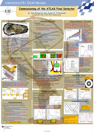
From ATLAS to Pixels: Mechanical Overview ATLAS • ATLAS Pixel Detector • Innermost tracking detector, surrounding beam pipe physicist 1.3 m 6 cm Detection of charged particles takes place in 1744 identicalATLAS Pixel Modules Pixel x46080 50 x 400 μm 1744 modules x 46080 pixels = 80 million channels! Sven Vahsen, LBNL
Pixel Project Overview • Pixel Detector is last sub-detector to be installed in ATLAS April 2007 as the 7m “Pixel Package”, which includes • Service panels (connections for electrical, optical, cooling) • Be beam pipe • Remaining work at CERN • Final stages of integration • Connection of service panels • Testing • Remaining slides • Overview of the pixel detector and how it works • Status of the project Trial insertion of pixel frame into support tube Sven Vahsen, LBNL
The LHC Tracking Challenge • ATLAS tracking : three sub-detectors from r = 5 cm - 1.2 m, inside 2T magnetic field. • Pixel Detector innermost highest granularity and radiation tolerance With pile-up at design luminosity H’bb interaction (36 sp) (3 sp) (4 sp) Only tracks with PT>1Gev, 0<h<0.7 shownOnly Si hits with 0<h<0.7 shownOnly TRT hits with Z>0 shown • Pixel Detector design constraints from LHC timing / event-environment physics, ATLAS design • Tracking in high multiplicity environment high granularity • Good impact parameter resolution high granularity + low mass • Distinguishing hits 25ns apart fast preamp rise time • 3.2 μs trigger latency (LVL2) on detector buffering of hits • High radiation dose low temp., high radiation tolerance Sven Vahsen, LBNL
The Pixel Detector Solution • Modules overlap on the support structure to provide hermetic coverage: 3 space points for |η|<2.5 for collisions up to 11 cm from nominal IP • 3 barrel layers at r = 5, 9, 12 cm • 2 endcaps with 3 layers • Will be first large-scale active pixel device in operation • i.e. ~ each pixel read out by dedicated preamp: 80 million channels • Approx. 10 kW operating power in active volume, at 2V • Detector will operate at -7°C • Cooling integrated into local support structure via thinned aluminum tubes, C3F8evaporation • Total mass is 10% X0 normal to beam 1.3 m Sven Vahsen, LBNL
The ATLAS Pixel Module • Kapton flex circuit: routes signals between FE and MCC. Routes LV (2V, 1.6V) to chips and HV (150-600V) to sensor • Sensor: where charged particles traversing detector liberate charge: 2 cm x 6 cm x 250 μm n bulk silicon rectangle, with 47,268 n+ pixels • 16 Front End (FE) chips: preamp channels, each connected to sensor pixels via bump bonding • Hits buffered for up to 3.2 μs (LVL2 latency) in “End Of Column” buffers on FE-chip • Upon LVL2 trigger, Module Control Chip (MCC) combines hits from FE chips into event • Data is read out electrically from module via 1m “Type 0” cable @ up to 160 Mb/s Solder bumps 50 μm ~ 2 x 6 cm • Data is converted between electrical and optical at far end of Type 0 cable Sven Vahsen, LBNL
The Pixel Detector Module • Sensor wafer • 16 FE chipsBump-bonded onto sensor 50 μm pitch Solder bumps • Electronics Design Work started ~ 10 years ago • Final version (Dec 2003) of FE chip is “FE-I3”: • 0.25 μm CMOS process, IBM, 3M transistors! Sven Vahsen, LBNL
Single Pixel: Detection of a Charged Particle • apply (150-600 V) reverse bias voltage • Free charge carriers (electrons & holes) are removed: silicon “depleted” • no incoming particles only leakage current < 1 nA / pixel • A passing charged particle at normal incidence liberated on average 22,000 electron-hole pairs per 300μm (~4fC) • charge swept towards bumps and into FE preamp by electric field, where it is converted to voltage pulse • charge typically shared by a few (1-3 pixels) Sven Vahsen, LBNL
In FE chip, charge-integrating amplifier converts charge pulse from sensor into voltage pulse Ouput voltage above threshold digital hit stored in EOC buffer Time over threshold (TOT) proportional to charge Information from hit ultimately preserved Bunch crossing ID (BCID) Time over threshold charge Pixel Geographical address The Pixel Preamp (single pixel) threshold Sensor / bump Q=CV • Digital controls for each pixel’s preamp threshold and more • Time over threshold (TOT) can improve position resolution in case of charge sharing: charge-weight each pixel Sven Vahsen, LBNL
Module Performance • Many test beam measurements: efficiency, timing properties, charge collection, spatial resolution • Results incorporated into ATLAS simulation/digitization • High efficiency and good timing characteristics even after irradiation Unirradiated 60MRad, ~1015n/cm2 Single pion test beam efficiency vs. trigger timing (10ns/DIV) Sven Vahsen, LBNL
Pixel Performance Tracking Performance • Pixel single-point resolution in r/phi • TDR: want < 13 μm • Test beam: • 7.5 μm before irradiation (at incidence angle 10o) • 9.7 μm after irradiation (at incidence angle 15o) • Determines resolution of transverse impact parameter, d0 (for b-tagging) • three tracking algorithms • “newTracking” takes full advantage TOT measurement to improve resolution in case of charge-sharing σ(d0) in μm • Simulation of single-muons, pT=200 GeV/c (low multiple scattering) • plot σ(d0generated – d0reconstructed) Sven Vahsen, LBNL
Module Production & Testing: Done! • Two commercial bump bonding vendors, six academic laboratories all running in parallel. • ~ 12 FTE technicians and 15 FTE physicists & students for 2 years. • Each individual pixel tested and characterized at intended operating temperature, -7°C • Preamp properties with internal injection circuit • Bump connectivity with 60-keV X-ray source • Built more modules than needed, ranked them by quality, discarded the worst 1744 Sven Vahsen, LBNL
Local supports: Staves and Sectors Highest-quality modules glued onto carbon support structures,which incorporate cooling tubes “Type0” cable “Staves” in barrel “Disk Sectors” in endcap (double sided) “pigtail” Al cooling tube Sven Vahsen, LBNL
Integration: Endcaps Done! • Sector Disk Endcap • Both endcaps completed in U.S. and shipped to CERN x8 x3 Three completed Pixel disks (one end-cap) with 6.6 M channels Sven Vahsen, LBNL
Geneva CERN: Volvo, back seat, lots of padding SFO Newark Geneva, Business class! Pixel Endcap C: Traveling in style! Sven Vahsen, LBNL
Endcap quality • Strict QC at all levels of integration • Bumps disconnecting when gluing modules on sector? • Increase in noise? • Placement precision? • Thermal performance? • Everything within spec! • Dead channels • Endcap C < ~0.2% • Endcap A slightly worse 3 modules need work • No noise increase • Placement precision of modules on sectors: 2.6 μm w.r.t. to target position in sector place 10-3 # MODULES # MODULES DEAD PIXELS PIXEL NOISE (e-) Sven Vahsen, LBNL
Integration: Barrels • 13 modules “loaded” onto each stave and tested at European institutes • Loaded staves then shipped to CERN for further integration, as shown here • Dedicated tooling developed to do carry out each integration stage safely Two staves bi-stave with cooling U-Link… Loaded half-shells clamped together Layer 2 …inserted into half-shells… Layer 1 B Layer Sven Vahsen, LBNL
Layer 2 completed on Sept 10 Pixel Layer2 – Half shell Pixel Layer2, after clamping Pixel Layer2, in Global Support Pixel Layer2, after clamping Layer2 used lowest-quality accepted barrel modules. Still only < 0.3% bad channels Sven Vahsen, LBNL
Integration of Remaining Barrel Layers • Layer1: finished last week (after pictures) • Expect to finish b-layer in ~ 3 weeks • Integrate all barrels and end-caps by the end of 2006 Pixel Layer1, 1st half-shell completed Pixel Layer1, 2nd half-shell. One bi-stave under test Sven Vahsen, LBNL
System Test and Cosmics • Final integration takes place in December, but endcaps already complete One endcap has been high-jacked for an 8% (6.6M of 80M channels) system test • Will exercise many production parts of system not mentioned in this talk • Services • DAQ • Control and interlock system • Use scintillators to trigger on vertical cosmics
The End Game • Jan-Feb 2007 devoted to Service Panel integration • If time left before installation (currently we have one month contingency) it could be used for cold test of whole pixel package • Insertion of pixel package into ATLAS in April 2007, followed by months of connecting, cabling, and testing • And then, hopefully, first LHC beam! Sven Vahsen, LBNL
Conclusion • Following nearly a decade of R&D, and years of production, Atlas Pixel Detector now in the final stages of integration • Both Endcaps complete and at CERN • Barrel L2, L1 complete, b-layer in a few weeks → 3 Layer Pixel Detector on schedule for installation in ATLAS in April 07!
Problems Overcome • cooling pipe corrosion • breaking cables
Tuning A Module • A module has 46 080 channels in 2 x 6 cm area, typically > 99.8% fully functional • Process variation across FE chips, preamps differ need “tuning” to make response of all pixels uniform • Each preamp has digitial “knobs” for tuning the preamp behavior, .e.g. • Tuning = find the settings for each pixel that give uniform response across module Adjust threshold of each pixel untuned module tuned module • In lab tests to date, typically tune to threshold of 4000 electrons • Well above typical noise of ~170 electrons • Modules work great, no stability issues! Sven Vahsen, LBNL
Actual ATLAS Pixel Sensor Bumps connect to implants • A diode junction forms wherever p-doped and n-doped regions touch. Depletion always begins at the diode junction as reverse external voltage is applied. • Hadron irradiation introduced p-type defects. Eventually this will cause the bulk to “type invert” and become p-type. At this point the diode junction shifts to the top. This was chosen on purpose because it allows to operate without fully depleting the bulk. • Leakage current increases drastically with irradiation! P-spray doping to isolate individual pixels Heavily n-doped pixel implants (doping too heavy to deplete) Diode junction Lightly n-doped bulk Guard rings Heavily p-doped back side contact Sven Vahsen, LBNL
Pixel Chip Front End Input from Pixel sensor (bump goes here) preamp comparator Sven Vahsen, LBNL
The MOS transistor schematic of the FE-I3 charge amplifier • Above is just one pixel! • 2880 pixels / readout chip ~3M (MOS) transistors / chip FE-I3). Sven Vahsen, LBNL
Front End Features • Programmable threshold = Global Threshold + Pixel Threshold • Calibration charge injection • Ability to measure leakage current • Time over Threshold (TOT) charge measurement • How long the red curve says above threshold depends on the size of the input charge Can easily change threshold for whole chip Can fine tune each pixel to compensate for response differences (Tuning) Input from detector V1 V2 switch Good old charge amplifier Injection capacitor (must be small) Sven Vahsen, LBNL