Download
1 / 13
130 likes | 154 Views
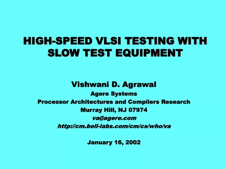
HIGH-SPEED VLSI TESTING WITH SLOW TEST EQUIPMENT. Vishwani D. Agrawal Agere Systems Processor Architectures and Compilers Research Murray Hill, NJ 07974 va@agere.com http://cm.bell-labs.com/cm/cs/who/va January 16, 2002. MEANING OF DELAY TEST. V1 V2. Transient region. Inputs.

E N D
HIGH-SPEED VLSI TESTING WITH SLOW TEST EQUIPMENT Vishwani D. Agrawal Agere Systems Processor Architectures and Compilers Research Murray Hill, NJ 07974 va@agere.com http://cm.bell-labs.com/cm/cs/who/va January 16, 2002
MEANING OF DELAY TEST V1 V2 Transient region Inputs Combinational logic Outputs Flip- flop Time Clock period Inputs and outputs synchronized with clock Agrawal: High-speed test
PROBLEM STATEMENT • Available automatic test equipment (ATE) speed is 100-200MHz; VLSI chip speed is 0.5-1GHz • No coverage of delay faults is obtained when ATE applies vectors and samples outputs at slow clock rate • A slow ATE can test delay faults in combinational circuits by skewing the output sampling times • Skewed output sampling method tests very few (mostly PI to PO) paths in sequential circuits • Problem: Develop a delay test method for slow ATEs that will give similar path coverage as obtained with an at-speed ATE Agrawal: High-speed test
PREVIOUS WORK • BIST (built-in self-test) with externally supplied high-speed clock (hardware overhead, non-functional paths tested) • ATE pin multiplexing (limited vector capability) • Reduced supply voltage, Wagner and McCluskey, ICCAD’85 (may change critical paths, reduce noise margins) • Latch designed to slow the circuit down in test mode, Agrawal and Chakraborty, US Patent 5,606,567 (1997), ITC’95 (needs special hardware, performance penalty) • Fast clocking of flip-flops with slow vector application and slow output sampling, Krstic, Cheng and Chakradhar, VTS’99 (low path coverage) Agrawal: High-speed test
A NEW METHOD • Given a vector-set with specific at-speed PDF coverage • Tester generates two clock signals: • Test-clock, N times slower than rated chip clock where N = test-speed reduction factor • Rated-clock, obtained by multiplexing N skewed test-clocks • (a) Apply vectors at test-clock speed • (b) Apply rated clock to flip-flops • (c) Synchronize output sampling with test-clock, using a skew, s = rated-clock period • Repeat steps (a)-(c) with skew = 2s, 3s, … Ns • Test application time (TAT) = N 2 x (at-speed TAT) Agrawal: High-speed test
TEST APPLICATION Speed reduction Factor, N = 4 Test inputs Primary inputs FF clock Output monitor strobes Application 1 Application 2 Application 3 Application 4 Agrawal: High-speed test
TESTING FOR FOUR TYPES OF PATHS PI PO I III IV II Path Types: I PI PO II FF FF III PI FF IV FF PO FF Agrawal: High-speed test
SOME PROPERTIES OF THE METHOD • All types of paths can be tested • Test application time (TAT) = N 2 x (at-speed TAT) • Coverage determined by simulation • Path-specific test generation possible Future detection State c’’ i1/o3 i1/o5 Non- detection i1/o1 i1/o2 i1/o3 State a State b State c i1/o5 V1=(i1,a) State d V2=(i1,b) i1/o4 State c’ Fault detected Agrawal: High-speed test
SIMULATED PDF COVERAGE s510 - 5,000 random vectors s5378 - 5,000 random vectors 50% At-speed ATE 40% Slow ATE 30% PDF Coverage 20% 10% 1 2 3 4 Slowdown factor (N) Agrawal: High-speed test
A LAB EXPERIMENT • Device: CD4029B (Texas Instruments) • Function: 4 bit binary/decimal presettable up/down counter • Package: 16 pin DIP • Gate count: 103 • Flip-flop count: 12 • I/O count: 9/5 • Clock frequency: 4MHz @5V • Tests: Fault coverage vectors from Gentest (90 vectors) • Path delay fault simulation for rated-speed operation and for high-speed test (Parodi et al., ITC’99) • Tests performed by C. Parodi and J. David at Holmdel using HP 82000/400MHz ATE Agrawal: High-speed test
RESULTS OF CD4029B TEST Three chips tested (A, B, and C) Maximum all-test-pass clock-rate (MHz) Vector application speed reduction factor, N Chips N=4 (1/4 speed) N=1 (At-speed) N=2 (Half-speed) A 3.922 4.367 3.937 B 4.367 4.167 4.167 4.132 4.115 4.367 C Simulation showed that slow testing perhaps activated paths that are longer than those activated by at-speed testing. Agrawal: High-speed test
A VLSI CHIP EXPERIMENT • BSM2 Chip: Boundary Scan Master Version 2 (Higgins and Srinivasan, VTS’00) • Agere 0.16 micron CMOS process • 65MHz clock @1.5V • Gate count: 18,823; Flip-flop count: 1,368; I/O count: 34/34 • Production Tests • 453,195 vectors, 96% coverage of stuck-at faults • 164,578 tested path faults (total 400 million paths) • Longest tested paths - 58 gates (longest physical path - 74 gates) • Path delay fault simulation for rated-speed operation (Parodi et al., ITC’99) • Functional Vectors: 68,608 • Rated-speed test fails above 85MHz • ½-speed test fails above 53MHz • ¼-speed test fails above 53MHz • 1/8-speed test fails above 53MHz Agrawal: High-speed test
CONCLUSION • It is possible to obtain same or higher PDF coverage with a slow ATE as with an at-speed ATE • A slow test-clock is used for input application and output monitoring • A rated-clock signal is applied to flip-flops; a slow ATE can generate fast rated-clock by pin multiplexing • Test application time (TAT) increases as square of speed reduction factor (N): TAT = N 2 x V where: V = number of vectors (for variable clock testing, TAT ~ N 2x V 2) • Test application time can be reduced by test optimization • Use PDF simulation • Generate path-specific tests • Proposed method only tests functional paths Agrawal: High-speed test