Download
1 / 24
240 likes | 483 Views
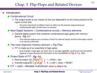
Flip-Flops and Related Devices. Wen-Hung Liao, Ph.D. 4/10/2002. Objectives. Recognize the various IEEE/ANSI flip-flop symbols. Use state transition diagrams to describe counter operation. Use flip-flops in synchronization circuits. Connect shift registers as data transfer circuits.

E N D
Flip-Flops and Related Devices Wen-Hung Liao, Ph.D. 4/10/2002
Objectives • Recognize the various IEEE/ANSI flip-flop symbols. • Use state transition diagrams to describe counter operation. • Use flip-flops in synchronization circuits. • Connect shift registers as data transfer circuits. • Employ flip-flops as frequency-division and counting circuits. • Understand the typical characteristics of Schmitt triggers. • Apply two different types of one-shots in circuit design. • Design a free-running oscillator using a 555 timer. • Recognize and predict the effects of clock skew on synchronous circuits. • Troubleshoot various types of flip-flop circuits. • Program a PLD using CUPL's state transition format for circuit description.
Clocked Flip-Flops • Controlled inputs + CLK • Setup and Hold times • Clocked S-C Flip-Flop • Clocked J-K Flip-Flop • Clocked D Flip-Flop
Setup and Hold times • Refer to Figure 5.16 • The setup time ts is the time interval immediately proceeding the active transition of the CLK signal during which the control input signal must be maintained at the proper level. • The hold time tH, is the time interval immediately following the active transition of the CLK signal during which the control input signal must be maintained at the proper level.
S-C Flip Flops • PGT S-C FF
Internal Circuitry of S-C FF • Consists of: • a basic NAND latch • a pulse steering circuit • an edge-detector circuit (Figure 5.20)
J-K Flip-Flop • J=K=1 does not result in an ambiguous output. • Goes to the opposite state instead.
Internal Circuitry of J-K FF • The only difference between J-K FF and S-C FF is that Q and Q’ outputs are fed back to the pulse-steering NAND gates. • Analyze the condition: J=K=1 and Qbefore=0
Clocked D Flip-flop • Has only one control input D, which stands for data. • Operation is simple: Q will go to the same state that is present on the D input when a PGT occurs at CLK. • In other words, the level presented at D will be stored in the FF at the instant the PGT occurs. • Application: Parallel Data Transfer Using D FF (P.203, Figure 5.26)
D Latch • D FF without the edge detector. • Has an enable input. (Figure 5-27) • Behave somewhat differently.
Asynchronous Inputs • Used to set the FF to the 1 state or clear to the 0 state at any time, regardless of the condition at the other inputs. (Figure 5.29) • Also known as override inputs.
IEEE/ANSI Symbols • D latch Q D C Q’ Enable
Flip-Flop Timing Considerations • Setup and hold time: for reliable FF triggering, minimum values are specified. • Propagation delays: the time the signal is applied to the time when output makes its change, maximum value is specified. • Maximum clocking frequency, f MAX: the highest frequency that can be applied to the CLK input of a FF and still have it trigger reliably.
Timing Considerations • Clock pulse HIGH and LOW times: the minimum time duration that the CLK must remain LOW before it goes HIGH, tw(L), and vice versa for tH(L). • Asynchronous active pulse width: the minimum time duration that a PRESET or CLEAR input must be kept in its active state in order to reliably set or clear the FF. • Clock transition times: for reliable triggering, the clock waveform transition times must be kept very short. • Actual ICS: 7474, 74LS112, 74C74, 74HC112
Potential Timing Problem • Refer to Figure 5-35, problem can occur when output of one FF is connected to the input of another FF, and both FFs are triggered by the same clock signal. • What if hold time requirement of Q2 is greater than propagation delay of Q1? • Fortunately, all modern edge-triggered FFs have very short tH, so there wouldn’t be a problem.
Master/Slave Flip-Flops • Used to solve the potential timing problem before the development of edge-triggered FFs with little or no hold-time requirement. • Can be treated as a negative-edge-triggered FF.
Flip-Flop Synchronization • Example 5-12 • Figure 5-37: asynchronous signal A can produce partial pulses at X. • Figure 5-38: Use edge-triggered D flip-flop to synchronize the enabling of the AND gate to the NGT of the clock.
More Flip-Flop Applications • Detecting an input sequence using J-K FFs. • Data storage and transfer: synchronous and asynchronous transfer • Parallel data transfer
Serial Data Transfer: Shift Register • A shift register is a group of FFs arranged so that the binary numbers stored in the FFs are shifted from one FF to the next the every clock pulse. • Refer to Figure 5-43 • Serial transfer between registers (Figure 5-44)
Frequency Division and Counting • J-K flip-flops wired as a three-bit binary counter • J=K=1 • frequency division: Using N flip-flops --> 1/2^N • counting operation • state transition diagram • MOD number
Microcomputer Application • Figure 5-48: example of a microprocessor transfer binary data to an external register.
Schmitt-Trigger Devices • A device that has a Schmitt-trigger type of input is designed to accept slow-changing signals and produce an output that has oscillation-free transitions. • See Figure 5-49, a Schmitt-trigger INVERTER
One-Shot • Has only one stable output state (normally Q=0, Q’=1), also known as monostable multivibrator • Once triggered, the output switches to the opposite state and remains in that ‘quasi-stable state’ for a fixed period of time, tp. • Non-retriggerable OS • Retriggerable OS
Analyzing Sequential Circuits • Step 1: Examine the circuit. Look for familiar components. • Step 2:Write down the logic levels present at each I/O prior to the occurrence of the first clock pulse. • Step 3:Using the initial conditions to determine the new states of each FFs in response to the first clock pulse. • Step 4: go back and repeat Steps 2,3 for the 2nd, 3rd…clock pulse